Search by Solutions
Product
Search
Observation and Inspection Solution
Contract Observation Service of semiconductor wafers for power devices using Transition High-Speed Observation Equipment
Although Mipox's observation is a non-destructive inspection, it evaluates threading dislocations with resolution equal to that of KOH etching and X-ray topography. With our proprietary phase processing technology and highly sensitive optical design, high precision analysis is possible. We provide "polarized light observation data of the whole wafer" and "threading dislocation density heat map", so that data such as the distribution of dislocations can be visualized and that feedback for yield improvement in crystal growth and subsequent processes becomes easy.
Service Contents
- Observation of threading dislocations in
semiconductor wafers and single crystal samples - Observation of internal strain in the wafer
- Observation of threading dislocations in the epi-wafer
- Visualization of dislocation distribution
Significance of Quality Evaluation of Semiconductor Wafer
In recent years, power semiconductor devices have garnered significant attention. Among them, attention has been particularly focused on crystal materials such as SiC (Silicon Carbide) and GaN (Gallium Nitride), and high-quality crystals to create wafers are being demanded. One of the indicators for defining quality then is threading dislocations. Threading dislocations contained in semiconductor wafers are considered to be one of the killer defects that cause performance degradation and yield degradation. Therefore, when manufacturing products with semiconductors, information such as the distribution and density of threading dislocations contained in wafers is very important.
Advanced polarized light observation - revolutionizing product quality
In the past, when measuring the distribution and density of threading dislocations accurately, large-scale measurement such as destructive testing like etching and X-ray topography with synchrotron light was required. However, it is difficult to use these evaluation methods steadily in manufacturing.
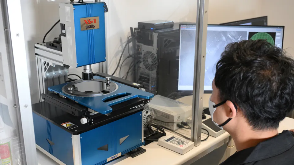
We developed XS-1 Sirius, a system for polarized light observation based on visible light using a high sensitivity optical design and our proprietary phase processing technology, as a system that can be easily used in the field of manufacturing while having resolution equal to the resolution of each of these evaluation methods.
In polarized light observation with XS-1 Sirius, threading dislocations can be evaluated with resolution equal to the resolution of evaluation of etch pit counts by KOH etching or dislocation observation by synchrotron light X-ray topography.

Observable samples
We can handle various types of semiconductor wafers and single crystal samples (SiC, GaN, diamond, AlN, sapphire, etc.). Although we recommend samples finished to a degree equal to or smoother than a mirror finish, we can start with contract polishing. Besides bulk wafers, wafers such as epitaxial wafers can be observed as well.
We will consider the necessity of processing from such factors as the surface condition. Feel free to consult with us.


Data to be provided in contract observation
- Data of polarized light observation of the whole wafer surface.
- Heat map of threading dislocation densities (low densities shown in blue and high densities shown in red)
Analysis of the type of threading dislocations
Contact the person in charge for individual consultation.
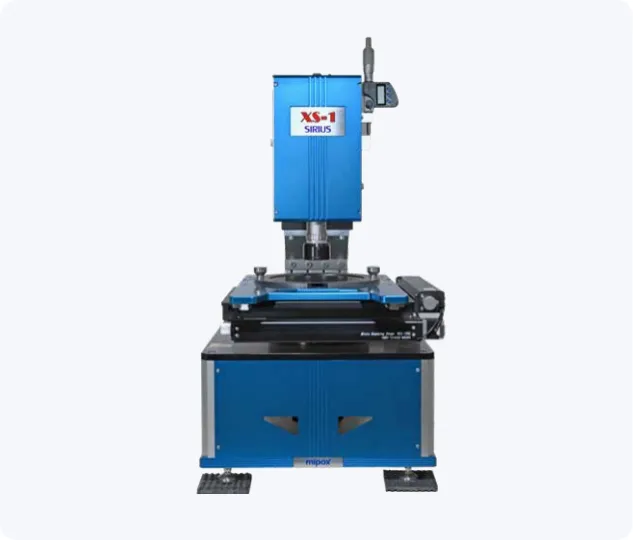
System (XS-1 Sirius) Specifications
Features of XS-1 Sirius
■ Groundbreaking crystal dislocation detection that replaces etching or X-ray topography made possible thanks to our propriety optical theory
■ No need for complicated adjustment, high-speed, high-accuracy observation made possible simply by setting a workpiece
■ Small and lightweight despite having a robust body structure, making labor saving for a footprint possible
Evaluation/Analysis Service
We also provide services to evaluate and analyze using our own equipment.
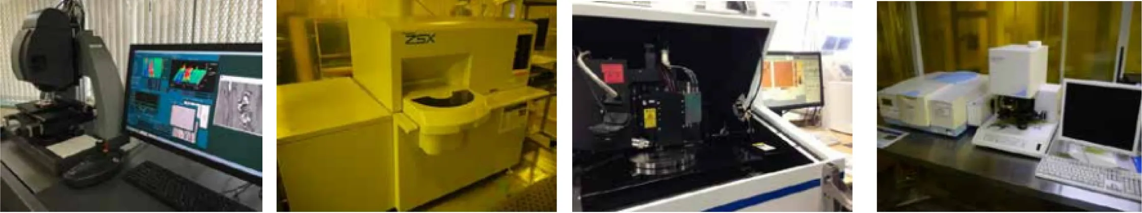
Equipment owned
- ・Fluorescence X-ray Analyzer
- ・X-ray Analyzer
- ・Optical Surface Analyzer
- ・FT-IR
- ・Laser Microscope (VK-9710)
- ・Laser Particle Size Analyzer
- ・Edge Profiler
- ・Thermal Analyzer
- ・SEM-EDX
- ・AFM L-Trace (Atomic Force Microscope)
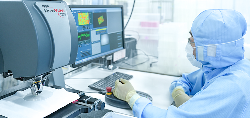
- ・Zygo 7100 (Three-dimensional Surface Analysis)
- ・Glass Strength Meter
- ・Roughness Meter (Contact, Non-contact)
- ・Particle Size Distribution (Microtrac X100,UPA, Electrical Resistance Method)
- ・Moisture Meter/Gloss Meter/Haze Meter/Microscope
- ・Surface Resistance Measurement/Thickness Gauge
- ・Viscometer (Type B,Handy,Process)
- ・Particle Counter (Airborne, Waterborne)
- ・DSC
- ・Film Thickness Meter
- ・White Light Interference Microscope
- ・Zeta Potential Meter
Q&A about Observation Service
What is the delivery time?
Please allow 1-2 weeks after order. If the quantity is large, please consult us separately.
Can I observe in person?
Currently, we are not accepting in-person observations. If we become capable of accepting in-person observations, we will let you know on this page.
Is it possible to rent the device?
We only accept contracted observations and do not rent out devices.
CONTACT
Mipox, the polishing professional, will propose the best polishing solutions, materials, and tools to meet your needs.
Please feel free to contact us.