Search by Solutions
Product
Search
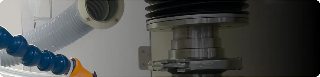
Wafer Coring / Resizing / Dicing
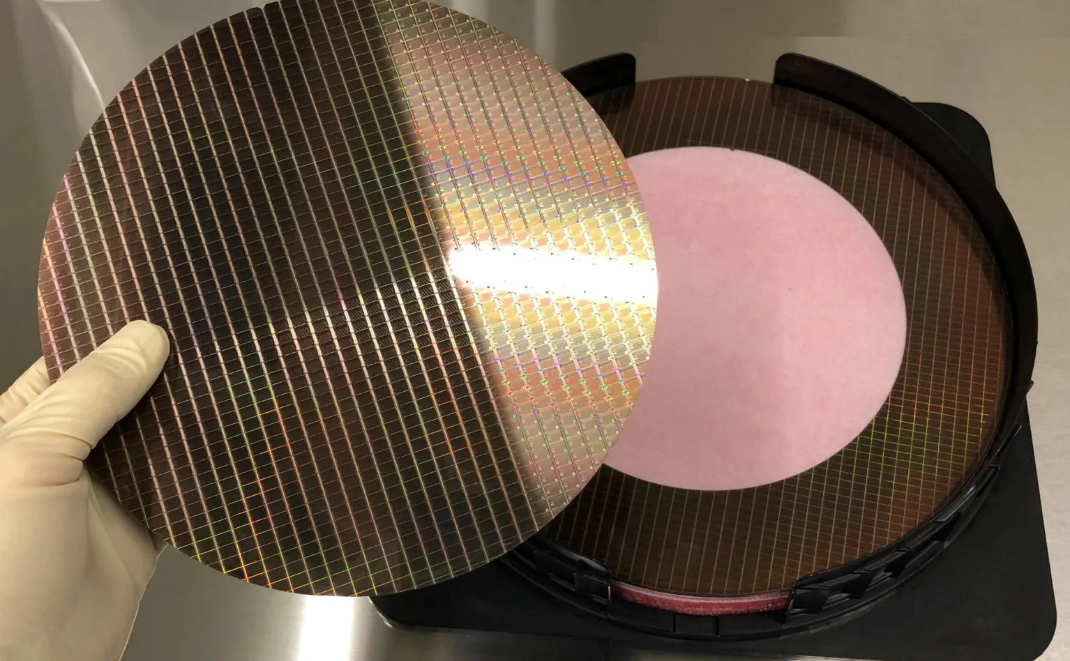
Mipox's Coring / Resizing
An appropriate cutting method is selected according to the state and application of an individual wafer. Low damage and high-quality resizing is offered.
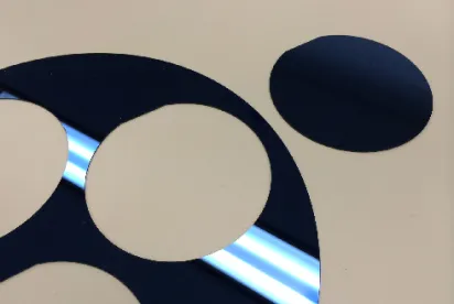
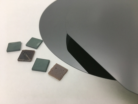
Wafer Coring / Size Reduction
We handle not only device-attached silicon wafers, but also compound semiconductors such as SiC wafers.
In addition, we also handle special format size reduction for such wafers as irregularly shaped wafers (half-inch wafers, chip shaped wafers).
From small lots for research and development applications to medium volume production - we handle a wide variety of wafer size reduction processes.
[Size reduction method]
• Laser cutting
• Waterjet cutting
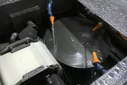
• Abrasive grinding method (such as blade, mounted grinding wheel, and core drill methods)
• Others


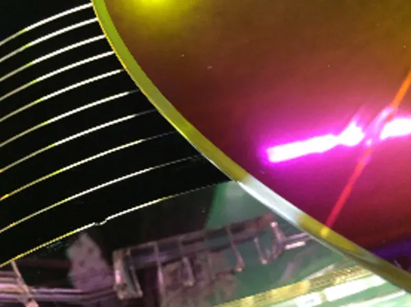
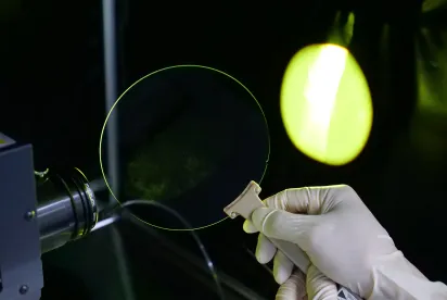
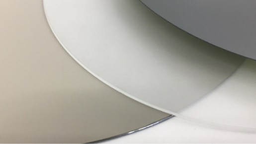
Chamfering after Resizing
Wafer edges and notches after resizing are very easily damaged, with many cutting marks of some kind remaining.
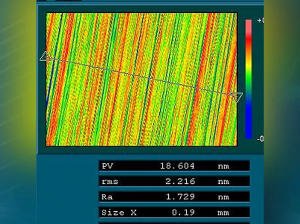
Mipox adopts a chamfering technique based on its proprietary polishing film method. Through low damage to wafers and adjustment to appropriate shapes and edge surface roughness, Mipox greatly contributes to yield improvement in the operation of resized wafers.
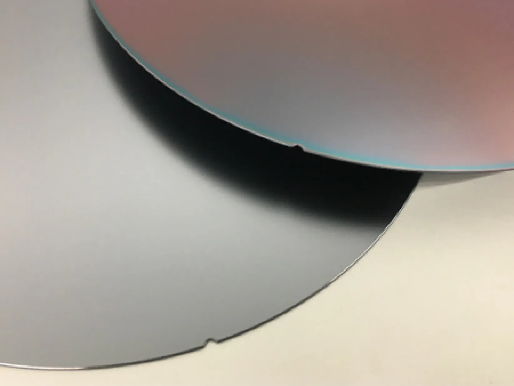
Notch polishing example
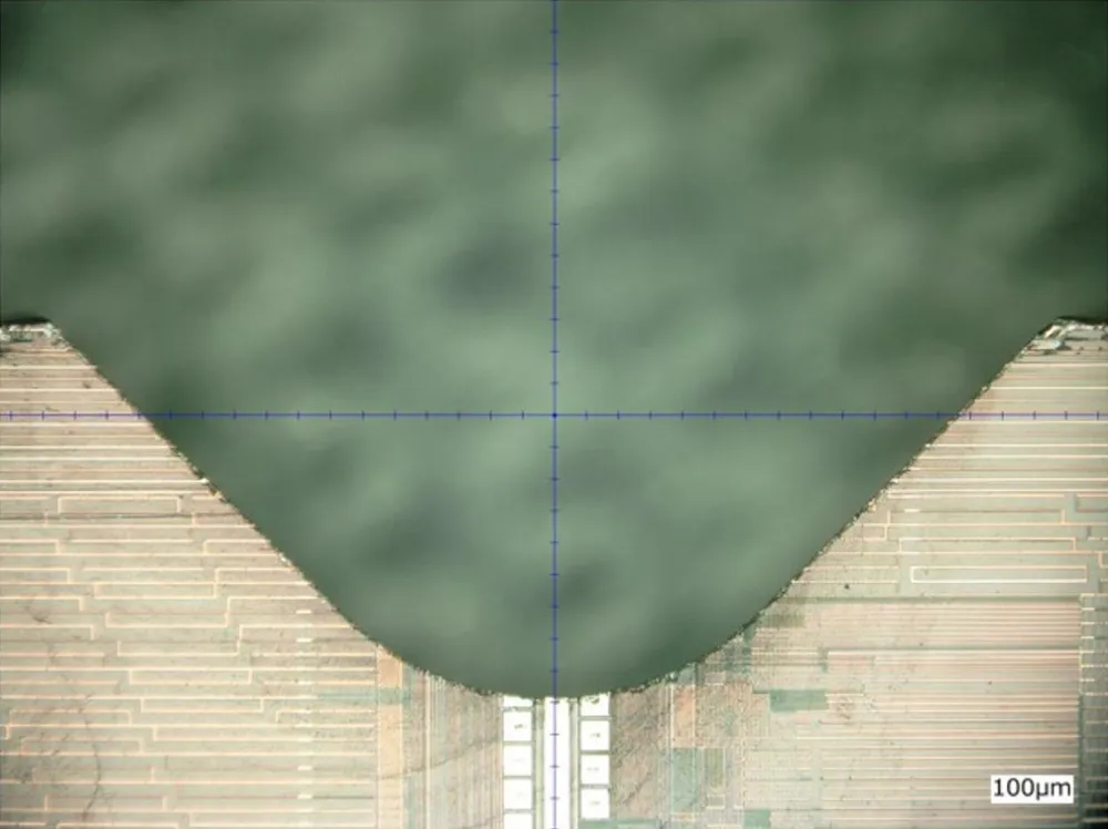
Before polishing: Wafer with chipping caused by cutting
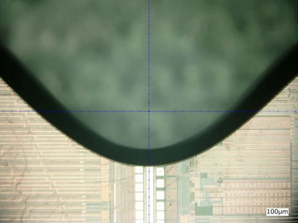
After polishing: Chamfering to improve strength
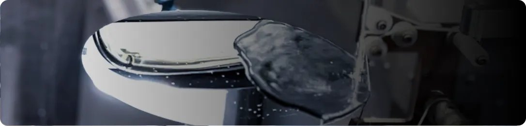
Terrace Processing
Taking advantage of one of the characteristics of the polishing film type polishing method - low damage to wafers, Mipox also handles wafer terrace polishing services.
Without causing damage to the epitaxial layer of a wafer with membranes such as GaNonSi, unnecessary membranes (unnecessary sections) can be removed and a mirror surface can be achieved. This process contributes to yield improvement in wafer manufacturing lines using the above type of wafer.
Process Flow
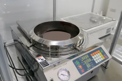
From acceptance inspection of wafers to surface protection (resist coating), cutting (coring), edge polishing, cleaning, and inspection - Mipox handles all the processes as a one-stop service.
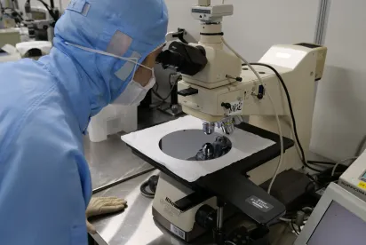
Acceptance Inspection
Resist Coating
Coring
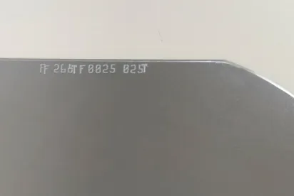
Laser Marking
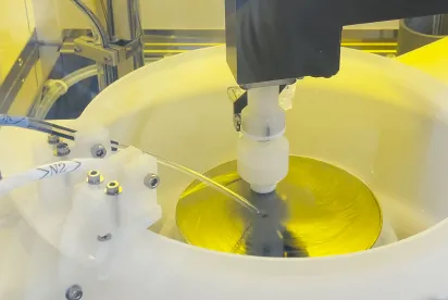
Edge Polishing
Resist Stripping
Cleaning
Pre-Shipment Inspection and Shipment
Inquiries about Precision Polishing Services
If you have any issues with precision polishing services, please feel free to consult us. Mipox, an expert in high-precision polishing, will propose solutions tailored to your challenges.
Mipox Technology Polishing Process Examples
Silicon Wafers
Compound Semiconductor Materials (Next-Generation Semiconductor Materials)
Fine Ceramics (Polycrystalline, Sintered, and Composite) Materials
Effective Edge Polishing Film for GaNonSi Challenges
CONTACT
Mipox, the polishing professional, will propose the best polishing solutions, materials, and tools to meet your needs.
Please feel free to contact us.