Search by Solutions
Product
Search
Compound Semiconductor Materials (Next-Generation Semiconductor Materials)
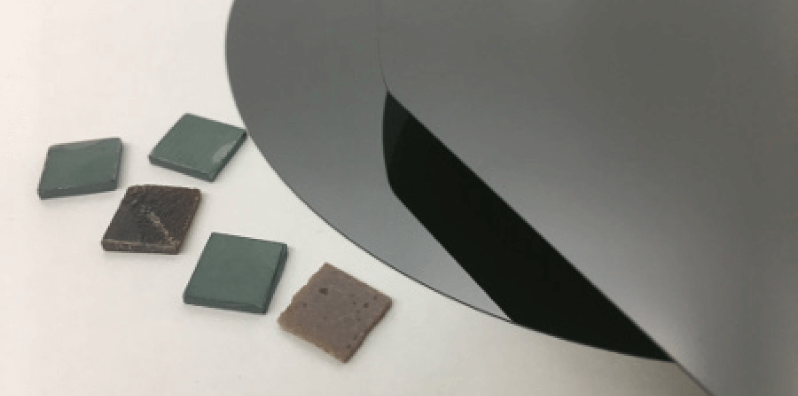
Table of Contents
Requirements for Compound Semiconductor Material Processing
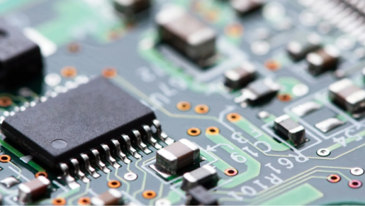
Compound semiconductors, primarily III-V group materials (including some oxide materials and diamond materials used for similar purposes) used in light-emitting devices, high-frequency (high-speed communication) devices, and power conversion devices, are expected to achieve many functions and performance levels unattainable with silicon (Si). In recent years, Mipox's contract polishing service has seen a rapid increase in requests for these applications.
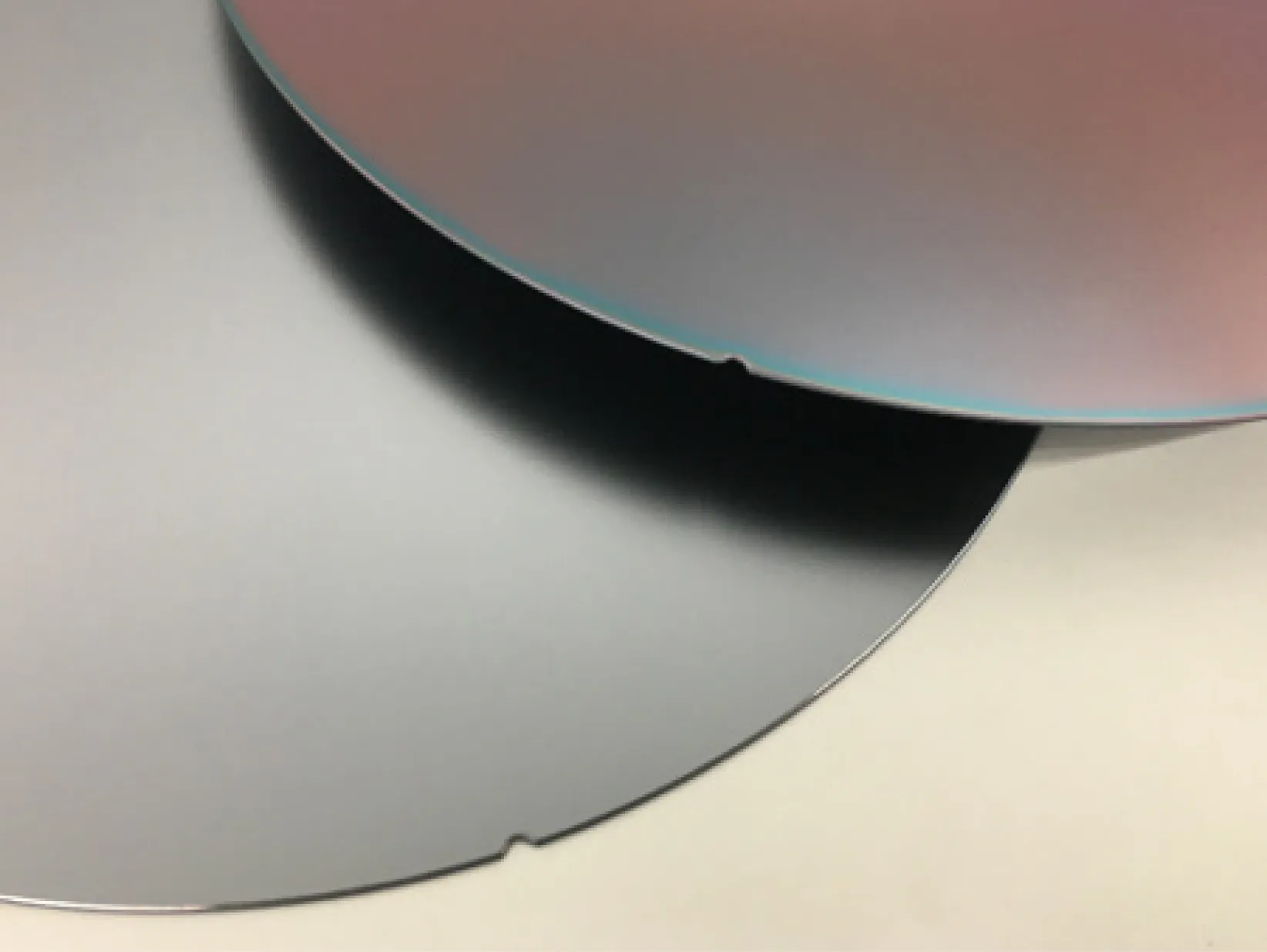
Particularly, diamond, hailed as the ultimate next-generation power semiconductor, boasts superior insulation breakdown voltage and ideal thermal conductivity (heat dissipation characteristics) compared to currently mainstream semiconductor materials such as Si, SiC, and GaN. As a result, various industries anticipate its realization (social implementation). While diamond is well-known as the hardest material among all substances, it paradoxically exhibits fragile physical properties such as being easily fractured or chipped. This makes it one of the most challenging materials to process into a usable state for semiconductor applications. However, the establishment of "diamond wafer edge treatment processing technology" using a proprietary "polishing film-based edge polishing method" has enabled rational edge processing, which has been incorporated into Mipox's contract polishing services.
Materials :
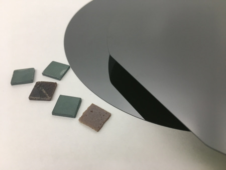
SiC, GaN, InP, GaP, GaAs, Ga2O3, GaSb, ZnS, ZnTe, C, etc.
Edge Polishing Applications
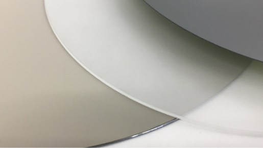
Mipox's contract polishing service specializes in edge chamfering and edge mirror (edge polishing) treatments, which are particularly effective in removing edge defects that cause problems during epitaxial film growth and mitigating their impact. Of course, we also handle rough and intermediate processing, such as chamfering after cutting out (size-down, inch-down) from normal large-diameter wafers. Using our proprietary polishing film method that minimizes damage such as chipping and slippage on wafers regardless of the material, we can accommodate various projects from small quantities to mass production.
Surface Polishing (CMP) Applications
From grinding, lapping finish (rough polishing, intermediate polishing) to CMP (epi-ready, bonding-ready) finish, we achieve the required precision using the optimal method for your application. We can handle CMP polishing of special-shaped substrates such as half-inch wafers, small pieces, and chip-shaped (broken wafers, etc.) substrates, as well as appropriate cleaning processes and quality inspections for each material.
Related Articles
Silicon Wafers
Compound Semiconductor Materials (Next-Generation Semiconductor Materials)
Fine Ceramics (Polycrystalline, Sintered, and Composite) Materials
Effective Edge Polishing Film for GaNonSi Challenges
CONTACT
Mipox, the polishing professional, will propose the best polishing solutions, materials, and tools to meet your needs.
Please feel free to contact us.