Search by Solutions
Product
Search
Effective Edge Polishing Film for GaNonSi Challenges
GaN substrates are being commercialized alongside SiC substrates as next-generation semiconductors. GaN-on-Si, which involves heteroepitaxial growth of GaN crystals on Si substrates, shows promising potential in terms of cost-effectiveness and performance, making it highly anticipated for practical applications. However, GaN-on-Si technology faces various technical challenges. In this context, we will explain how Mipox's polishing film-based edge polishing technology effectively addresses the technical issues of GaN-on-Si wafers using innovative techniques.
Table of Contents
GaN as a Next-Generation Semiconductor
Gallium Nitride (GaN) is a semiconductor material used in power semiconductors, LED lighting, and high-frequency devices. Along with Silicon Carbide (SiC), it has long been anticipated as a next-generation semiconductor material. Recently, GaN has become commonplace in AC adapters for computers and smartphones, contributing to the proliferation of USB Power Delivery standards and enabling fast charging, high output, and miniaturization.
What is GaNonSi?
GaNonSi (Gallium Nitride-on-Silicon) technology involves heteroepitaxial growth of GaN on Si wafers. This technique offers the potential for mass production and significant cost reduction in manufacturing high-power devices. Major power semiconductor manufacturers worldwide are actively developing GaNonSi technology, with frequent announcements of prototypes and manufacturing line implementations.
Advantages of GaNonSi Substrates
Compared to single-crystal bulk GaN wafers, which are typically limited to 2-3 inches in diameter, GaNonSi allows for easy manufacturing of large-diameter substrates (6-8 inches, 12 inches). It also enables the utilization of existing Si device manufacturing lines without the need for new investments in small-diameter single-crystal bulk GaN-specific equipment.
| Specification | GaN | GaNonSi |
|---|---|---|
| Diameter | 2-3 inches | 6-8 inches, 12 inches |
| Equipment Investment | Required | Not required |
Technical Challenges of GaNonSi Substrates
Despite its advantages, GaNonSi substrates face several technical challenges:
- 1. High tensile stress due to thermal expansion coefficient mismatch between GaN and Si
- Susceptibility to breakage from minor impacts, especially at the edges
- Risk of Ga contamination in semiconductor manufacturing equipment
- Difficulty in applying conventional etching techniques for GaN removal
Countermeasures for Common GaN-on-Si Technical Challenges
To address the technical challenges of GaN-on-Si, the following measures are often implemented.
- Utilizing non-standard, extremely thick Si wafers to mitigate overall wafer warpage after GaN epitaxy
- When sourcing non-standard thick Si wafers is difficult, downsizing from larger diameter substrates to secure adequate thickness
- Post-GaN epitaxy size reduction processing to remove the periphery of GaN-on-Si, which is prone to defect formation
While these countermeasures can be expected to have some effect on GaN-on-Si technical issues, the use of non-standard Si wafers often precludes edge treatment (chamfering and mirror polishing). Furthermore, the sharp and rough edges that appear after size reduction processing can have a detrimental impact on the structural integrity of GaN-on-Si wafers. Consequently, the benefits of these measures are typically not realized or are difficult to achieve.
To address these technical challenges, Mipox's film-based edge polishing technology offers the following characteristics, which prove effective in resolving GaN-on-Si technical issues.
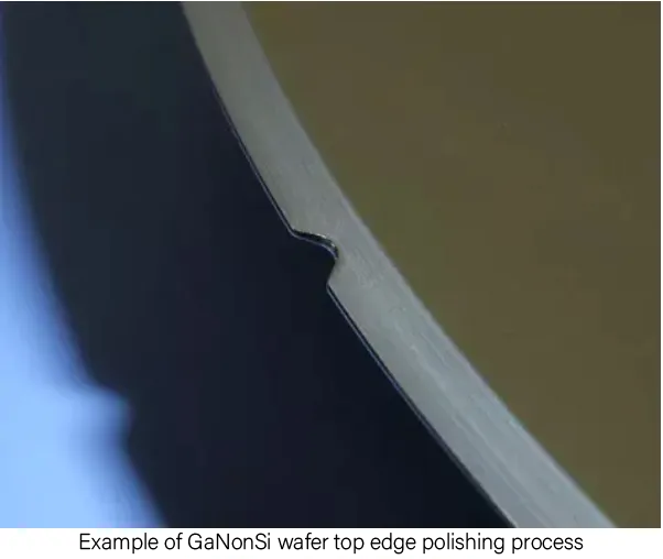
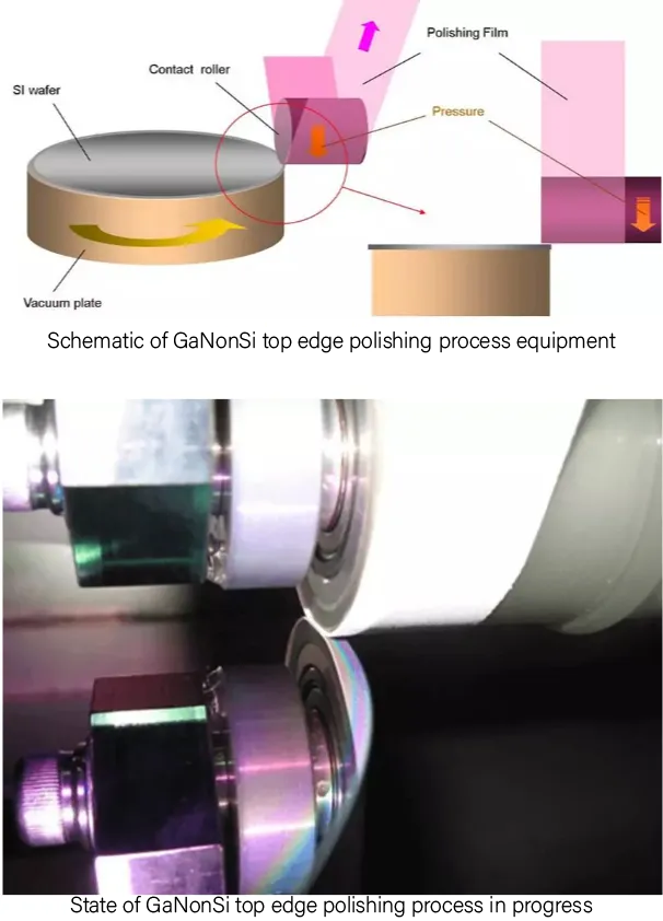
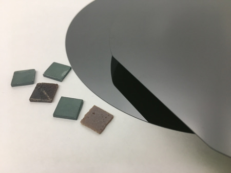
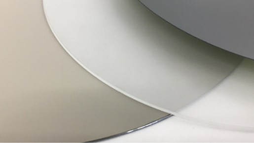
Mipox's Film Polishing Edge Polish Technology for GaNonSi Challenges
- Low-damage edge removal, chamfering, and mirror finishing of GaNonSi substrates
- Flexible edge treatment for ultra-thick Si substrates used for warpage control
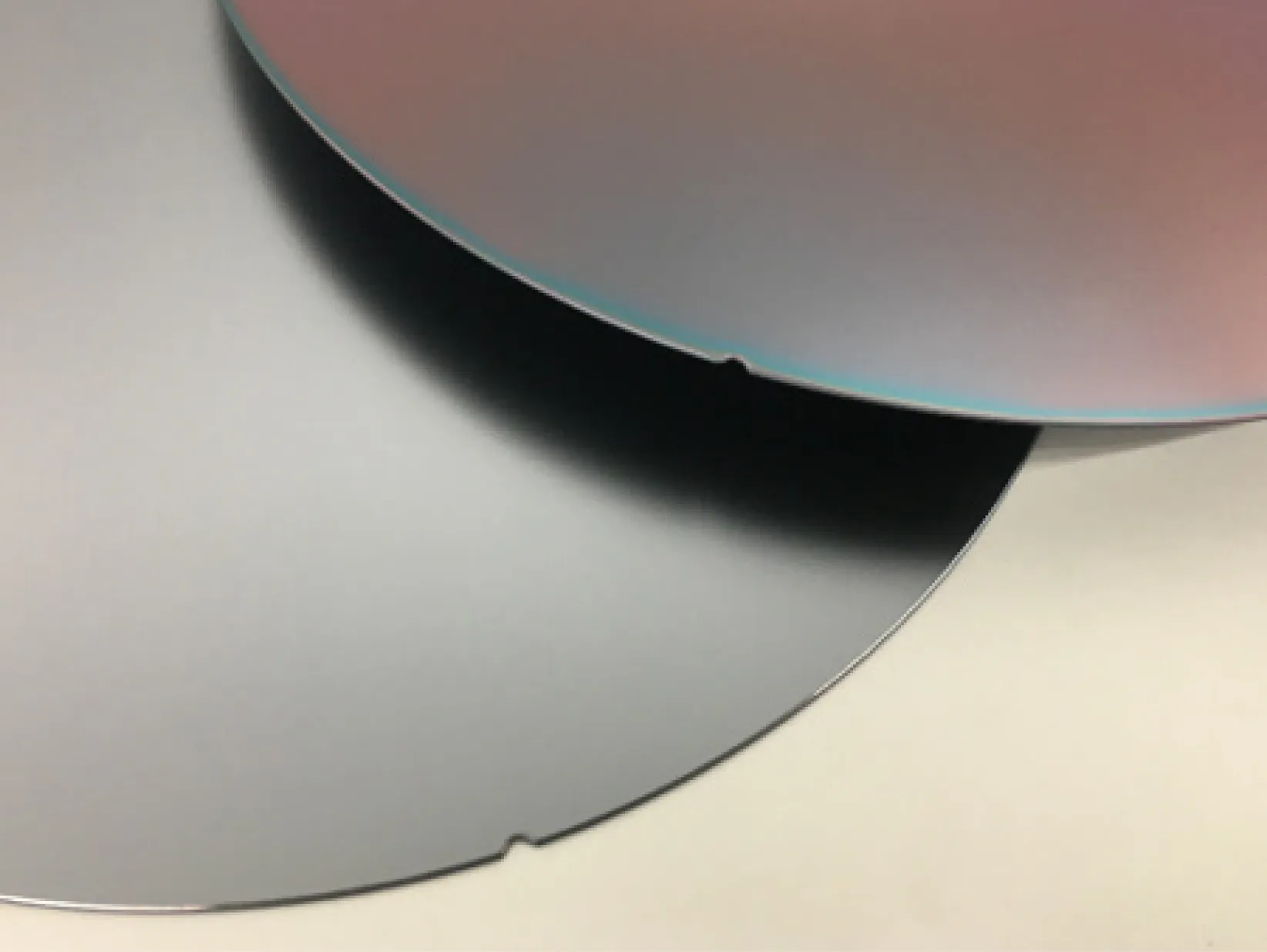
- Easy GaN removal at notch areas
- Simultaneous removal of all constituent films, including buffer layers
- Simple post-processing cleaning due to the use of only polishing film and pure water
- No special chemical treatments required, making it process-agnostic
- Low risk of slip occurrence in GaN films (including underlying SiC films) during 12-inch to 8-inch size reduction, ensuring stable yield
While these countermeasures can be expected to have some effect on GaN-on-Si technical issues, the use of non-standard Si wafers often precludes edge treatment (chamfering and mirror polishing). Furthermore, the sharp and rough edges that appear after size reduction processing can have a detrimental impact on the structural integrity of GaN-on-Si wafers. Consequently, the benefits of these measures are typically not realized or are difficult to achieve.
To address these technical challenges, Mipox's film-based edge polishing technology offers the following characteristics, which prove effective in resolving GaN-on-Si technical issues.
Conclusion
Mipox's film polishing edge polish technology is widely adopted for GaNonSi substrates due to its ability to easily remove various films strongly adhered to Si wafer edges through mechanical action. Additionally, it offers edge mirror treatment (polishing), which enhances particle re-adhesion prevention, GaNonSi substrate strength, damage prevention, and yield improvement. We encourage you to utilize Mipox's "Film Polishing Edge Polish Technology" for your future GaNonSi substrate operations.
Related Articles
Silicon Wafers
Compound Semiconductor Materials (Next-Generation Semiconductor Materials)
Fine Ceramics (Polycrystalline, Sintered, and Composite) Materials
Effective Edge Polishing Film for GaNonSi Challenges
CONTACT
Mipox, the polishing professional, will propose the best polishing solutions, materials, and tools to meet your needs.
Please feel free to contact us.