Search by Solutions
Product
Search
Wafer Making Services
Wafer Making (Substrate Manufacturing)
Mipox offers a one-stop wafer making service (substrate manufacturing service) covering all wafer manufacturing processes for ingots (crystal blocks and base materials) of various materials.
Wafer Making (Wafering)
Mipox's polishing service offers a one-stop wafer making service (substrate manufacturing service) centered on Mipox's proprietary edge polishing technology and planar polishing technology with extensive experience in processing difficult-to-machine materials.
Boules (ingots) are received from customers, and through Mipox's one-stop service, they are processed into completed wafers that meet the customers' quality requirements.
We, Mipox, have a good track record in the field of wafer making, especially in ceramic materials, and receive inquiries for wafer making in combination with such processes as room temperature bonding and thinning that are the subsequent processes.
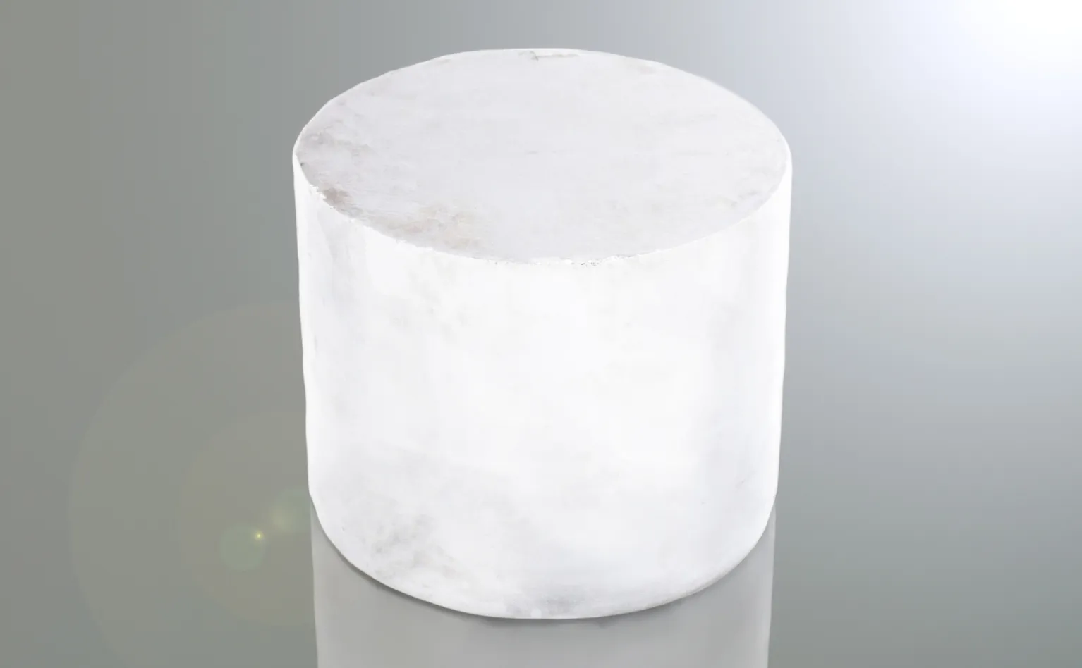
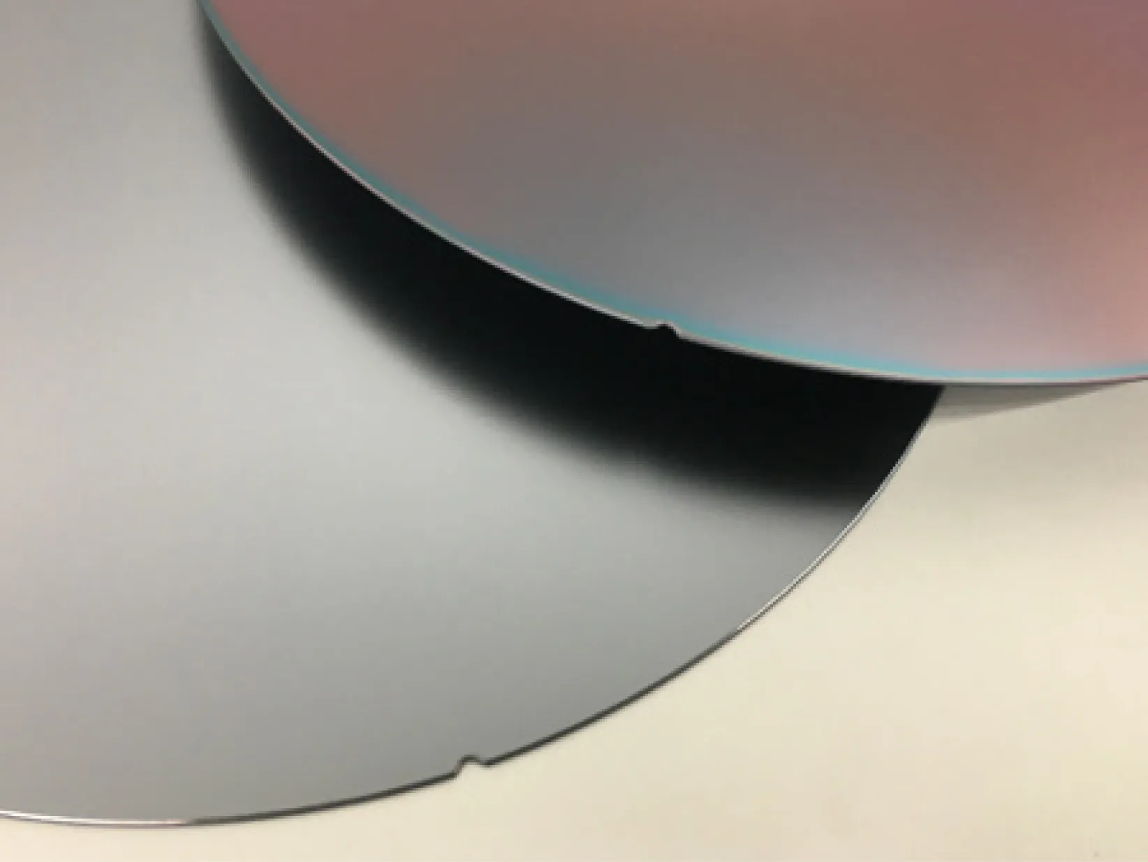
Ingots
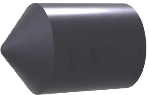
Slicing

Wafering

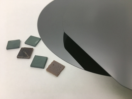
Wafer Making Example Ultra-High Precision Planar Polishing of Ceramic Materials (Sintered Body, etc.)
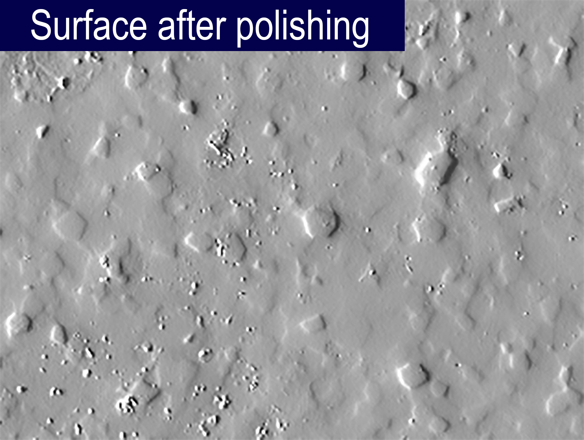
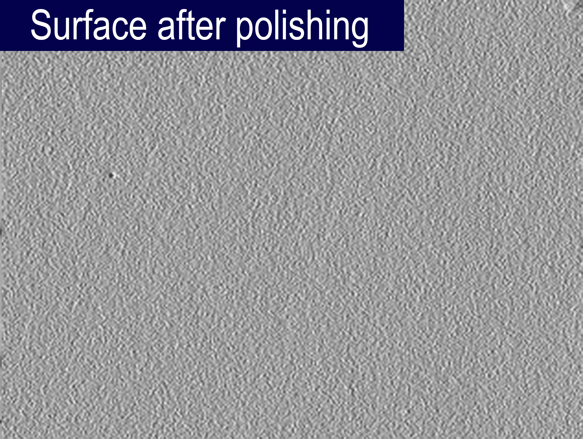
For various ceramic materials (sintered body, polycrystalline materials) whose planarization has been considered to be difficult, we can achieve a higher level of precision surface roughness (elimination of crystal grain steps).
The elimination of crystal grain steps is expected to bring many benefits, such as reduced voiding and improved bonding strength in the subsequent bonding treatment process, improvements in heat sink performance, and enhanced optical characteristics.
Applicable Substrates
PolySiC, AlN, SiC, Al2O3/YAG and other polycrystalline and sintered bodies. Processing target examples - Ceramic materials such as SiC, AlN, SiN, Al2O3/YAG, MgAl2O4, GaN (CVD-manufactured, polycrystalline, sintered bodies)
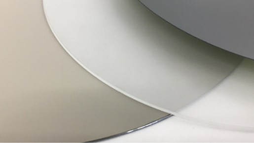
Surface Polishing of Sintered Body
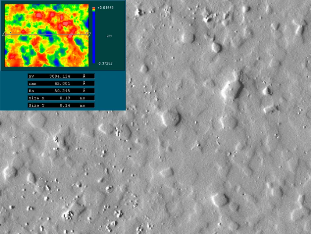
Conventional Ceramic Material Polished Surface
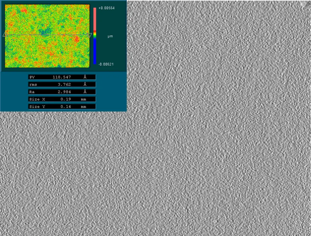
Surface Condition After Mipox Polishing Treatment
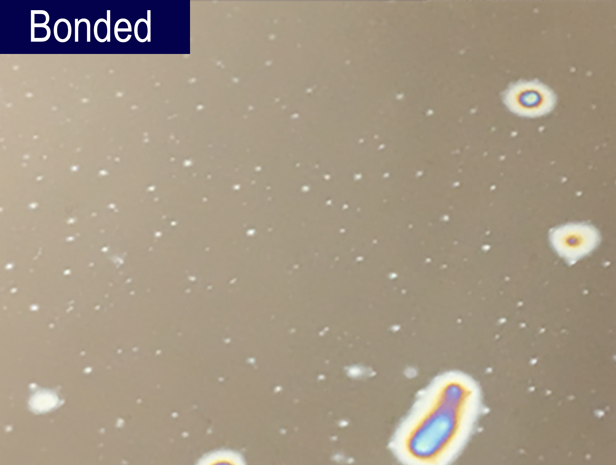
Wafer Making Example Room Temperature Bonding of Different Materials, Void-free Bonding
Taking advantage of our proprietary ultra-high precision planar polishing technology, we provide the bonding of different materials by using various ceramic materials that have until now been considered to be difficult to be bonded, and high-quality room temperature bonding services that keep void formation to an absolute minimum that was previously unavoidable due to material-related issues such as gaps and voids.
Besides SEMI standard wafers (up to 6 inches), we flexibly handle wafers of different sizes in diameter and chip-shaped substrates of several millimeters as well. We also have an ultra-high precision alignment mechanism (positioning mechanism) with as low as ±0.2μm bonding accuracy, thus meeting various bonding needs.
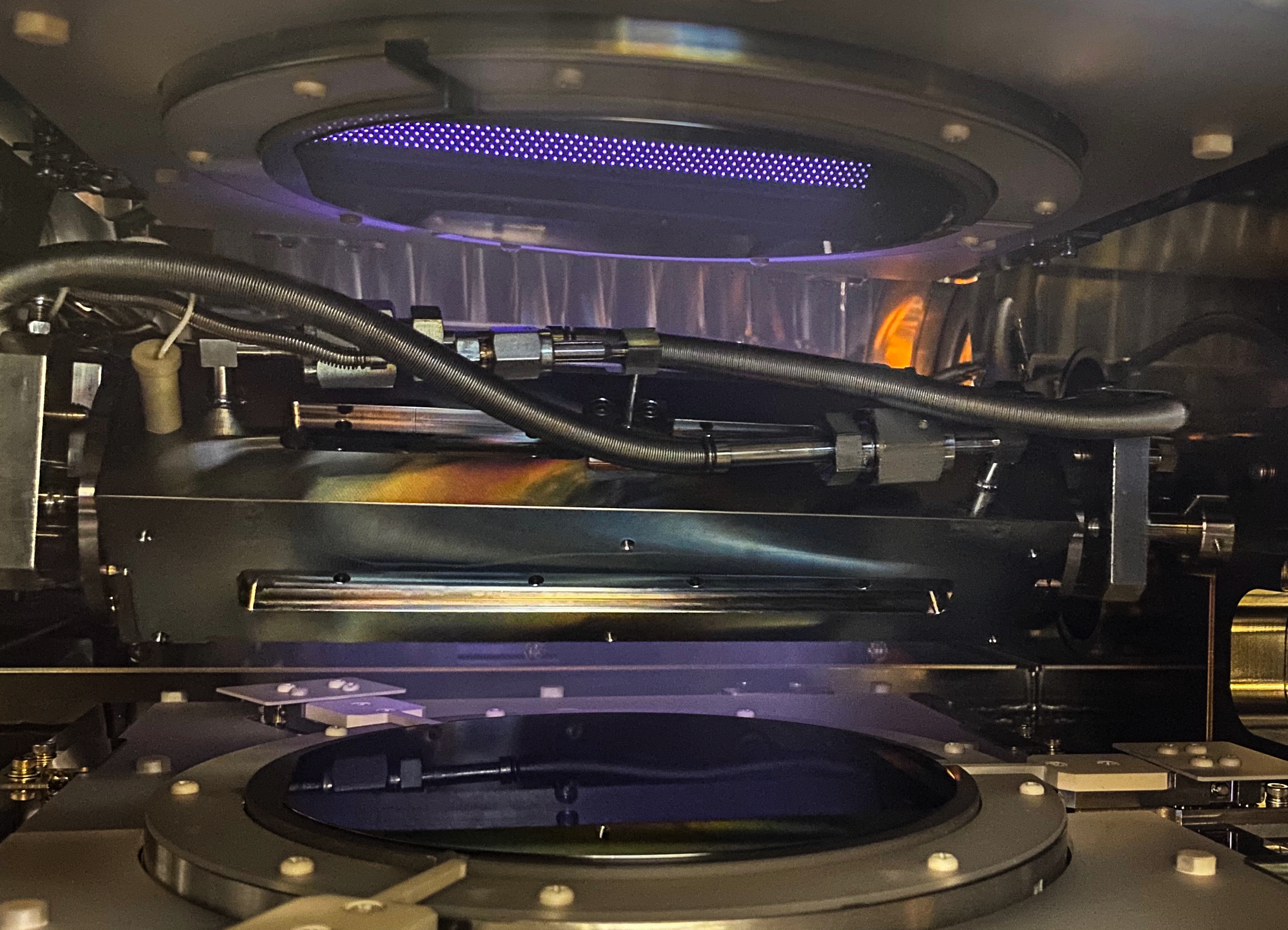
Mipox Owned Bonding Equipment
Correlation Between Surface Roughness and Bonding Interface
Other
Mipox

Mipox Technology Polishing Process Examples
Silicon Wafers
Compound Semiconductor Materials (Next-Generation Semiconductor Materials)
Fine Ceramics (Polycrystalline, Sintered, and Composite) Materials
Effective Edge Polishing Film for GaNonSi Challenges
CONTACT
Mipox, the polishing professional, will propose the best polishing solutions, materials, and tools to meet your needs.
Please feel free to contact us.