Search by Solutions
Product
Search
Room-Temperature Wafer Bonding
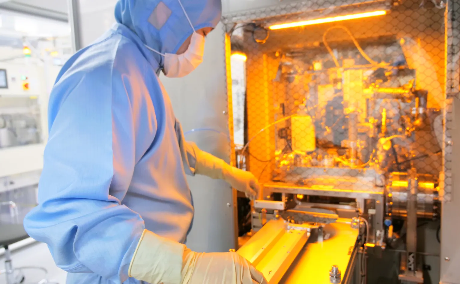
Room Temperature Wafer Bonding
Room temperature bonding is a technology that bonds different materials without applying heat. By activating the material surface in an ultra-high vacuum environment, high-quality bonding without being affected by thermal expansion can be realized even between different materials.
Mipox's room temperature bonding service handles projects combining silicon wafers, compound semiconductor wafers, oxide wafers, ceramic material wafers, and others, with a focus on prototyping for power semiconductor applications, surface wave filter applications, high frequency devices, various MEMS and LED applications.
Requirements for Wafer Room Temperature Bonding
Relationship between Surface Roughness and Bonding Technology
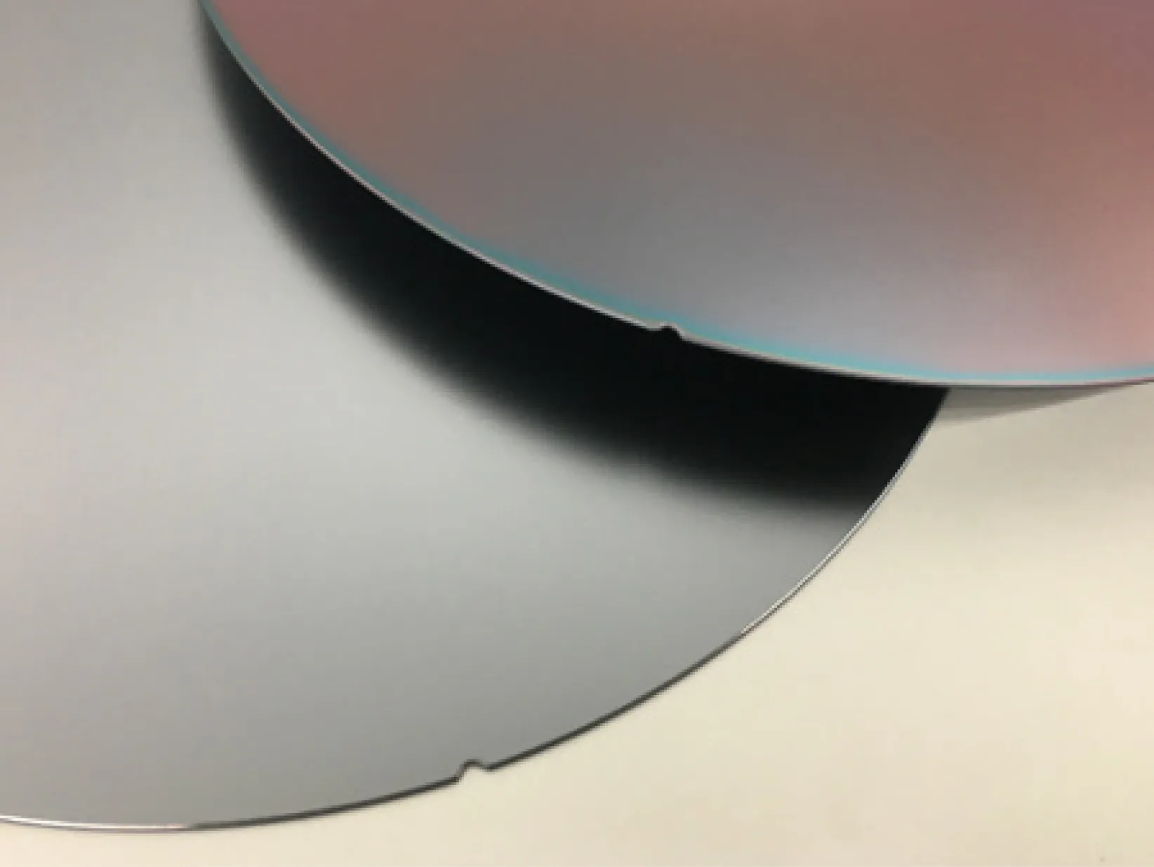
Wafer bonding is a very delicate process; even microscopic irregularities and foreign objects as small as several nanometers (nm) could be a direct cause of failures such as void formations and bonding strength insufficiencies. In most cases, it is desirable that the surfaces of wafers to be bonded should be as smooth as possible; in a method such as polishing (CMP), accuracy of an arithmetic average surface roughness of around 0.2nm (Ra) is required.
In addition, "roll-off" near the wafer edge can be a significant cause in deteriorating the bonding result, so high-level polishing technology suppressing such roll-off becomes necessary.
Achievement of Ultimate Surface Roughness
Mipox realizes high-quality bonding by applying its proprietary polishing that creates the ultimate in surface roughness to materials used for room-temperature bonding.
Ultra-high precision surface roughness is created for materials normally considered to be difficult to polish (difficult-to-machine materials), such as compound (e.g., SiC, GaN) semiconductor substrates, single-crystal diamond substrates, and polycrystalline (sintered body) (e.g., SiN and AlN) materials. We have achieved a breakthrough in the application to materials traditionally considered to be difficult to bond.
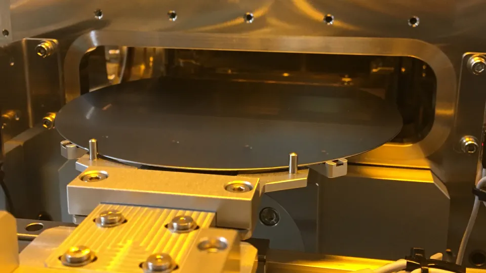
Ultra-High Precision Alignment Room-Temperature Bonding
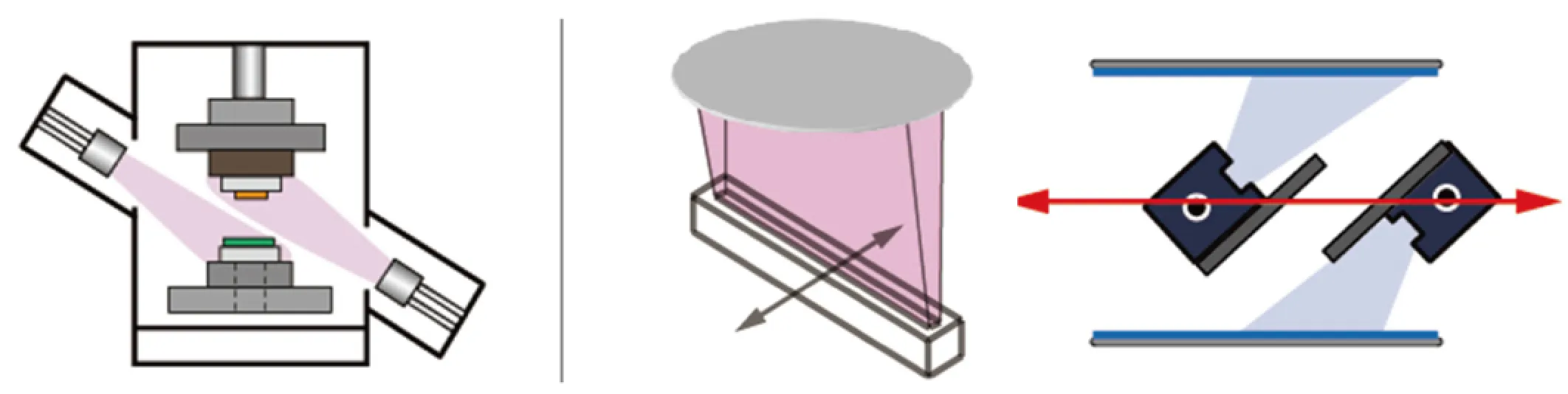
Mipox's room-temperature bonding equipment recognizes the position of an infrared (IR) transmission image with high precision, and is compatible with ±0.2μm ultra-high precision alignment bonding that uses a piezo actuator (a positioning element to which the piezoelectric effect is applied) performing position control in the directions of six axes.
The common alignment method for bonding, which aligns wafers only in the planar direction, has a limit to its accuracy (±1.0-0.5μm) because some misregistration occurs when wafers contact each other. Our ultra-high precision alignment room-temperature bonding far surpasses this accuracy and can suppress misregistration within ±0.2μm.
Wafer Room Temperature Bonding Techniques
Mipox's wafer room-temperature bonding services target 4-inch and 6-inch wafers, but can also support 3-inch or less small wafers, irregularly shaped wafers, half-inch size wafers, and others.
* Note that a dedicated jig or holder may need to be created depending on the wafer size or shape. Please consult us in advance.
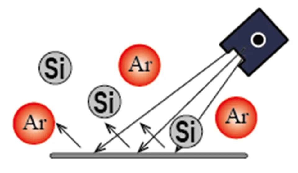
Direct Room Temperature Bonding with Argon Bombardment in Ultra-High Vacuum
Our room-temperature bonding equipment is compatible with "Si-FAB", a bonding method that irradiates Si atoms simultaneously at the time of Ar (argon) or N2 (nitrogen) beam irradiation.
A Si-rich surface can be formed without excessive Si deposition on the bonding surface. Even in electrode-containing bonding, insulation can be secured.
This bonding method is widely used for SiC (silicon carbide) wafer bonding, whose application examples have been increasing in recent years.
Nano-Adhesion Bonding
Normally, room-temperature bonding does not support ionic crystalline materials. However, as a method complimenting that point, a bonding method using Si sputtering, which puts an interlayer between wafers, is available (nano-adhesion bonding).
By introducing less than one layer of Si atoms on the interface, it becomes possible to bond even ionic crystalline materials well. Since nano-adhesion bonding can realize the bonding of combinations of diverse materials, it contributes to the expansion of bonding applications.
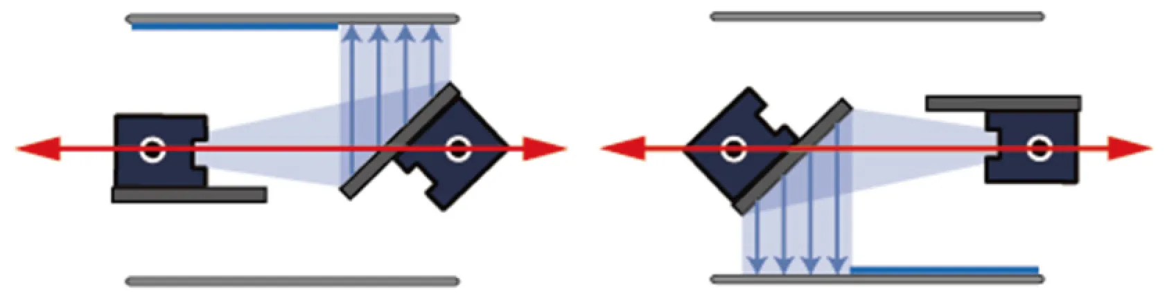
Room-Temperature Bonding Adopting a Movable Ar Beam Source Method
Fixed Ar beam sources, which have existed for many years, could not uniformly activate the entire wafer surface. Mipox solved this problem by adopting a scannable, movable Ar beam source. High-quality bonding is achieved from the center to the periphery of a wafer with within-wafer variations in bonding strength kept to a minimum.
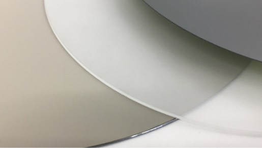
Wafer Room-Temperature Bonding Process Example
Planarization (CMP)
Polish the planar surfaces of wafers of different materials to obtain the surface roughness and flatness required for room-temperature bonding.
Precision Cleaning
Remove particles and contaminants on the wafer planar surface.
Inspection
With the appearance inspection equipment "Micro-MAX", conduct a final check to see whether scratches or dirt that causes problems with bonding remains on the wafer surface.
Bonding
Bond wafers of two different materials under their appropriate room-temperature bonding conditions. Check the bonding result (bonding state) with a tool such as an infrared camera.
Edge Polishing
Polish the areas near the edges of the bonded wafer to prevent chipping and damage.
Planar Polishing
Perform thinning (planar grinding and polishing (CMP)) on the bonded wafer.
Mipox Technology Polishing Process Examples
Silicon Wafers
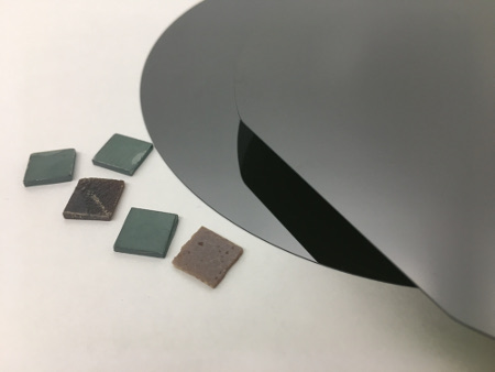
Compound Semiconductor Materials (Next-Generation Semiconductor Materials)
Fine Ceramics (Polycrystalline, Sintered, and Composite) Materials
Effective Edge Polishing Film for GaNonSi Challenges
CONTACT
Mipox, the polishing professional, will propose the best polishing solutions, materials, and tools to meet your needs.
Please feel free to contact us.