Search by Solutions
Product
Search
Planar Polishing (CMP) and Slurry
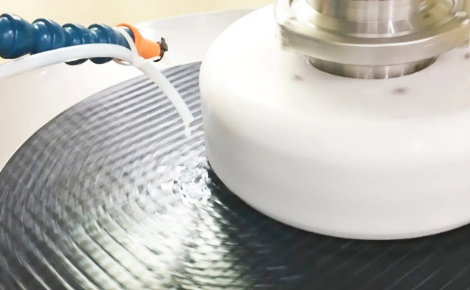
Planar Polishing (CMP)
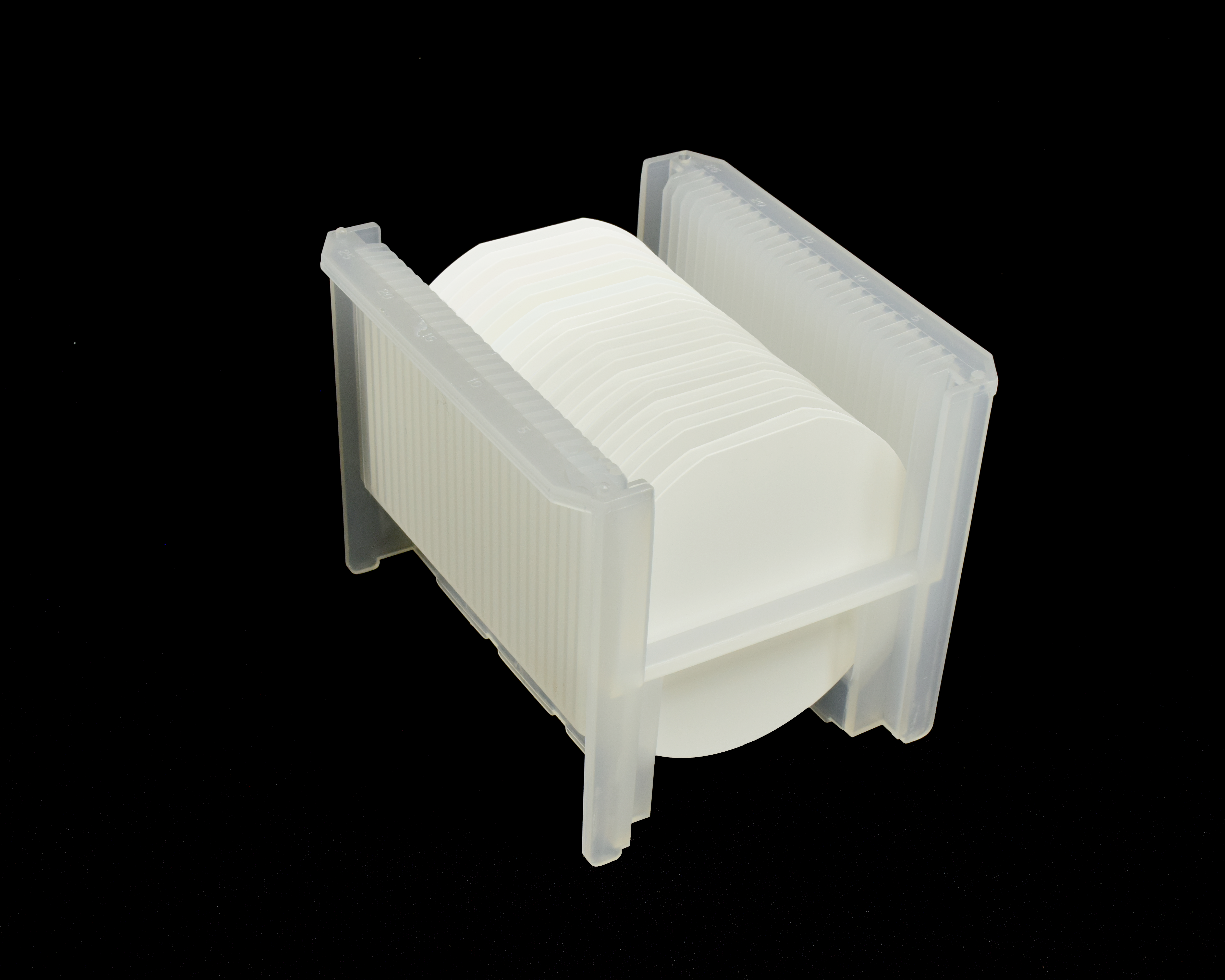
Mipox's planar polishing (CMP) covers a wide range of applications, from planar polishing of various wafers (substrates) to CMP of insulating films, metal films, resin films, and others. We can handle substrates from small and chip sized ones to SEMI standard 12-inch wafers.
CMP Process
We respond to customer requirements for such items as material properties, surface roughness, thickness dimensions (warpage, etc.), and cleanliness. A wide range of applications are supported - from medium-volume production to small-lot testing (process development, prototype development).
In addition to CMP processes, we can also handle precision cleaning and room-temperature bonding, which are placed in the subsequent processes.
CMP Process Examples
- Single Crystal
- Film Thickness Control
- Damascene (embedding process)
- Polycrystalline
- Roughness Improvement
- Hybrid Bonding
- Sintered Materials
- Wafer Step Elimination
Compatible with Various Materials
Mipox's polishing service supports a wide variety of polishing targets. We not only handle common semiconductor materials such as single-crystal silicon and various compound materials, but also actively support composite materials, organic materials, and new materials being developed for various applications.
Especially, we have extensive experience with ceramic materials (sintered body, polycrystalline material applications). Ceramic material applications are typical applications that play a core role in our polishing service with many examples of technical breakthroughs.
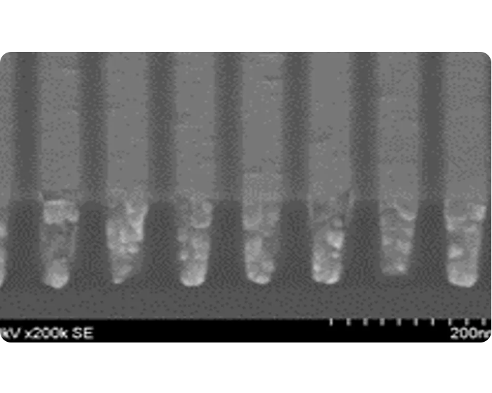
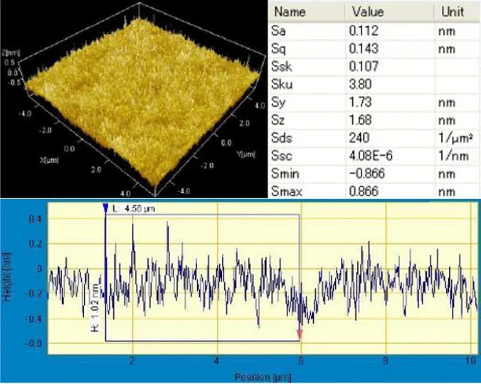
Achieving Ultimate Surface Roughness
Mipox creates ultra-high precision surface roughness for materials normally considered to be difficult to polish (difficult-to-machine materials), ranging from SiC, GaN, and other compound semiconductor substrates to SiN, AlN, MgO/Al2O3, and other polycrystalline ceramic materials.
In addition, since we possess precision measurement equipment such as ZYGO and AFM as well as the visual inspection system "Macro-Max", we can accurately grasp surface conditions.
By combining polishing film type planar polishing equipment equipped with proprietary mechanisms such as oscillation and head rotation mechanisms and our polishing films, we can handle grinding levels from high-rate polishing to mirror finishing, and realize wafer surfaces suitable for bonding.
Materials with Proven Track Records
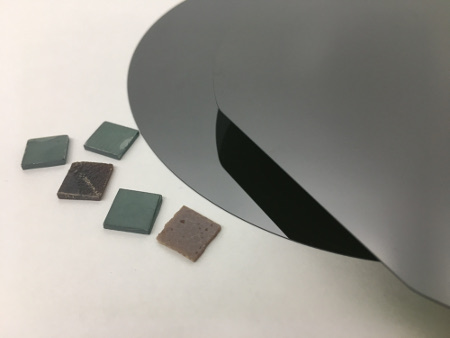
Ceramic Materials, Sintered Body, Polycrystalline Materials
Ceramic materials including SiC (Silicon Carbide), AlN (Aluminum Nitride), Si3N4 (Silicon Nitride), Al2O3 (Aluminum Oxide), YAG (Yttrium Aluminum Garnet), PZT (Lead Zirconate Titanate), and composite materials such as MgAl2O4.
Metal Films
Cu (Copper), Al (Aluminum), Au (Gold), Pt (Platinum), Ru (Ruthenium), Mo (Molybdenum), Ni (Nickel), Ag (Silver), Ti (Titanium), W (Tungsten), Fe-Ni (Iron-Nickel alloy), Ni-P (Nickel-Phosphorus alloy), Cr (Chromium) and other plated surfaces.
Examples of Materials: Ceramic Materials, Sintered Body, Polycrystalline Materials
For various ceramic materials (sintered body, polycrystalline materials) whose planarization has been considered to be difficult until now, we can achieve a higher level of precision surface roughness (elimination of crystal grain steps).
The elimination of crystal grain steps is expected to bring many benefits such as reduced voiding and improved bonding strength in the subsequent bonding treatment process, improvements in heat sink performance, and enhanced optical characteristics.
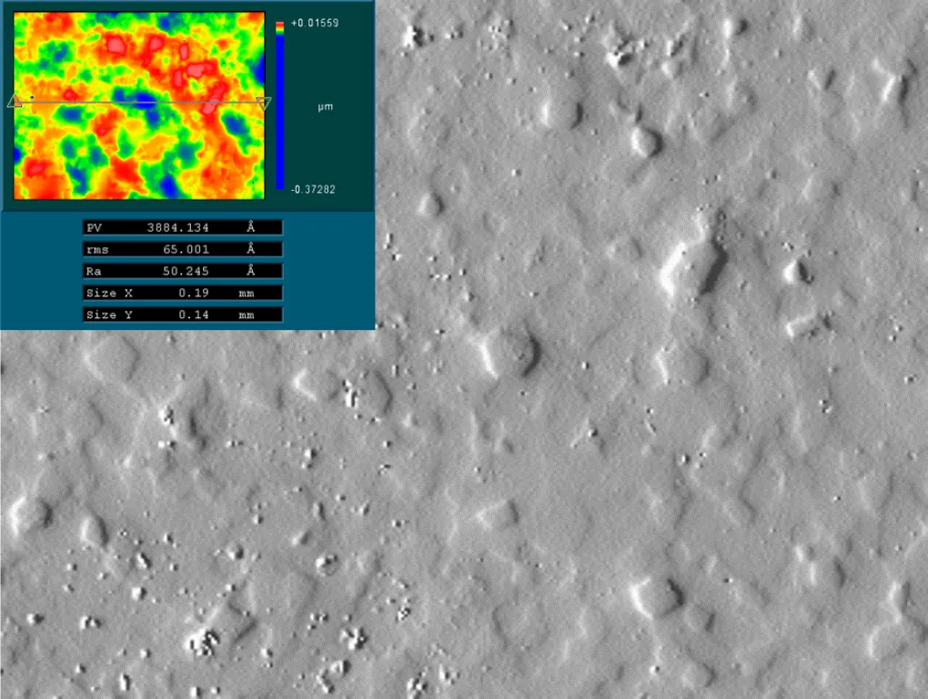
Conventional ceramic material polished surface
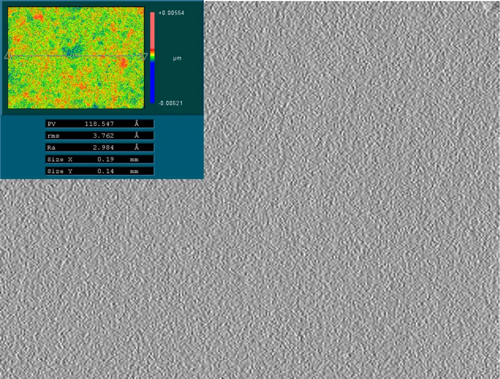
Ceramic material surface condition after
Mipox's polishing treatment
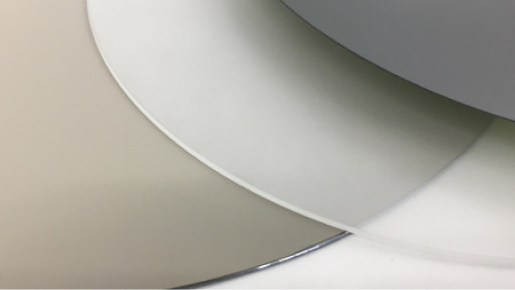
Slurry
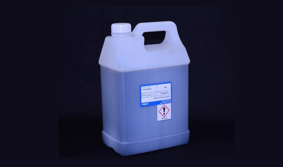
Slurries for Difficult-to-Machine Materials
Taking advantage of the mixing technology cultivated in our polishing film manufacturing, we produce dedicated slurries in-house mainly for polishing services. We create customized products by arranging abrasive grains and chemicals suitable for processing targets provided by customers.
Upon request, we will apply these slurries to customers' manufacturing lines at the time of process transfer (technology transfer). In addition to developing dedicated slurries for our polishing services, we also provide (sell) some slurries independently. We also respond to requests for special products not available in the product lineup of other slurry manufacturers and small-quantity orders.
Mipox Technology Polishing Process Examples
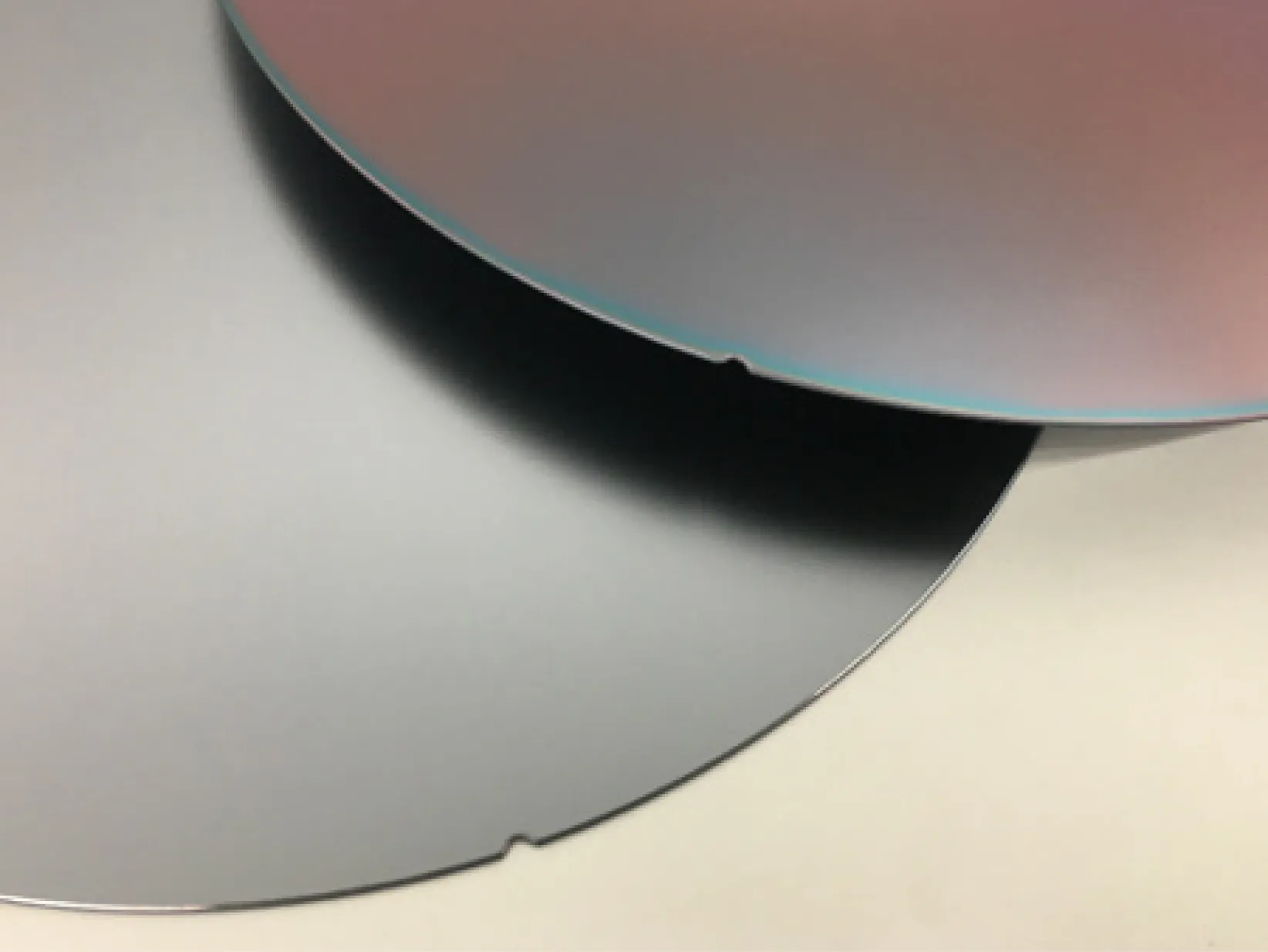
Silicon Wafers
Compound Semiconductor Materials (Next-Generation Semiconductor Materials)
Fine Ceramics (Polycrystalline, Sintered, and Composite) Materials
Effective Edge Polishing Film for GaNonSi Challenges
CONTACT
Mipox, the polishing professional, will propose the best polishing solutions, materials, and tools to meet your needs.
Please feel free to contact us.