Search by Solutions
Product
Search
Precision Polishing Services
Mipox Precision Polishing Services
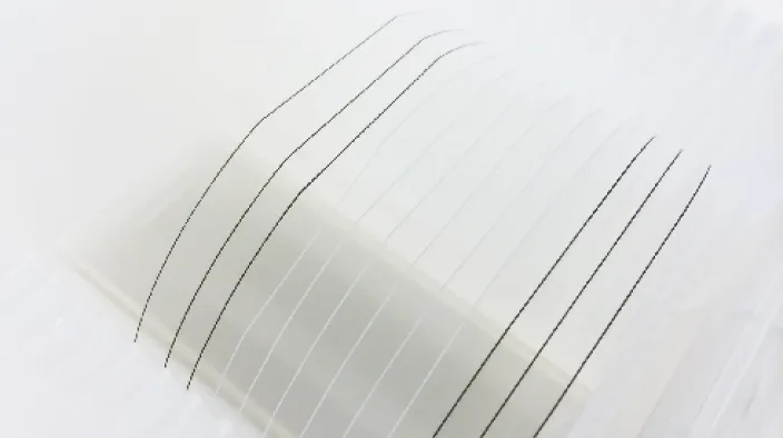
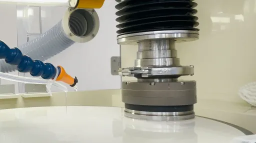
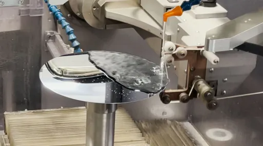
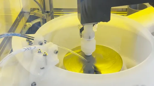
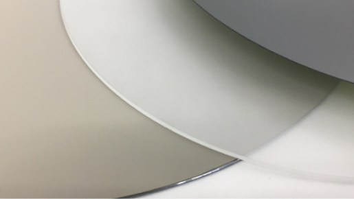
By applying our high-precision polishing technology that has been cultivated over many years, Mipox offers one-stop solution type contract polishing, cleaning, and bonding services for semiconductor wafers (such as crystal substrates, ceramic substrates, and substrates for devices), semiconductor-related components, and others.
Our in-house abrasives (such as polishing films and CMP slurries) and dedicated polishing equipment are put to full use to flexibly respond to requirements from a single process to wafer making covering reception of ingots to all processes.
If requested, we can respond to contract process development and technology transfer (process transfer) as well. We provide support so that transfer to the customer’s mass production line or in-house manufacturing can be carried out smoothly.

One-Stop Solution
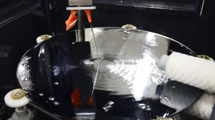
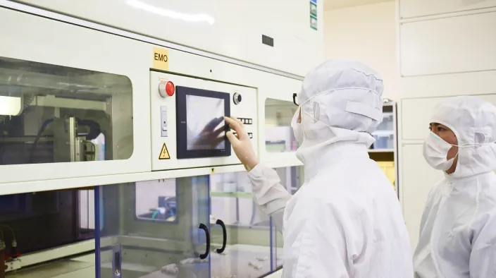
Applying our precision polishing technology cultivated through "Polishing", which is one of Mipox's core technologies, we provide a "one-stop solution service" centered on semiconductor wafer applications. We can undertake the tasks of prototyping, development manufacturing, and small to medium volume production.
Wafer manufacturing processes (such as a polishing process) are collectively managed by Mipox to arrange rational manufacturing processes. We meet customer requirements with appropriate quality standards and delivery times.
Common Customer Challenges
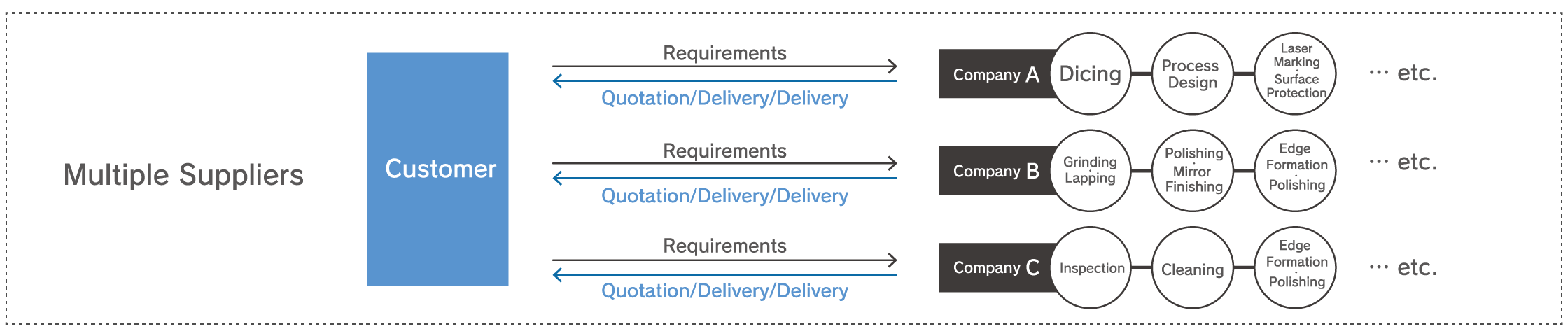
Mipox's One-Stop Solution
Mipox proposes optimal manufacturing processes.
To meet customers' requirements, we make full use of internal and external resources to arrange manufacturing processes. Appropriate processes will be proposed.
Customers can obtain completed products (such as wafers) satisfying their requirements with just one request.
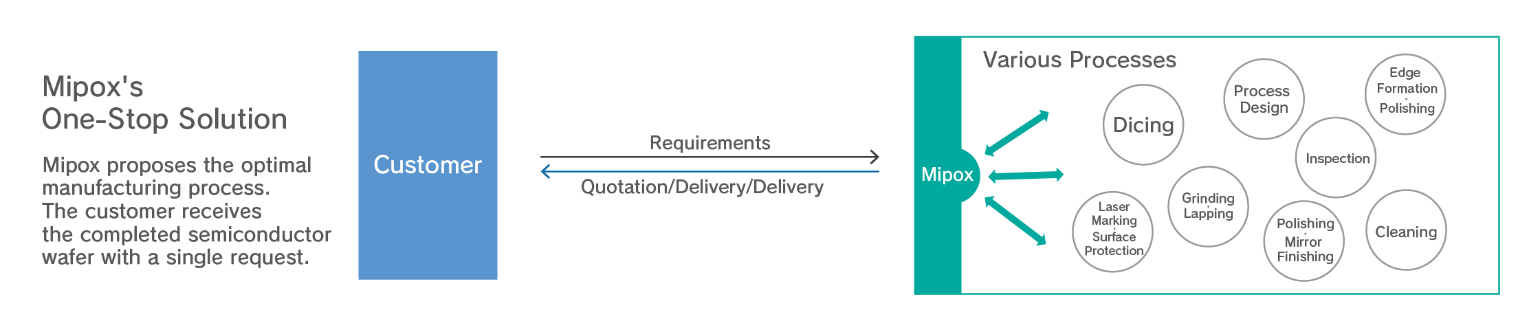
Normally, when considering outsourcing semiconductor wafer manufacturing, complicated tasks such as quote requests, delivery time adjustments, and schedule management are required for each contractor that handles each manufacturing process.
Mipox's One-Stop Solution collectively manages these tasks, thus reducing the customers' burden and arranging rational manufacturing processes from the viewpoints of quality, delivery time, and cost.
Flow to High-Precision Precision Polishing Services Contract
Inquiry
Inquiries are accepted through the website contact form.
Consultation
Our sales representatives or technical department staff will discuss your requirements. Confidentiality agreements will be signed according to the project content and circumstances.
Specification Definition
A series of processing specifications will be discussed. Specifications may be defined after prototyping and evaluation.
Prototyping & Evaluation
A series of processing operations (prototyping) will be conducted according to the contract content and specifications.
Mass Trial Production
Specifications will be determined by reflecting trial results and assuming mass production. A system that meets the customer's requirements in terms of quality, delivery, and cost will be built.
Contract Agreement
Start of Mass Production
Process Development and Transfer Flow
Inquiry
Inquiries are accepted through the website contact form.
Consultation
Our sales representatives or technical department staff will discuss your requirements. Confidentiality agreements will be signed according to the project content and circumstances.
Prototyping and Evaluation
A series of processing operations (prototyping) will be conducted in accordance with the contract content and specifications.
Specification Definition
A series of processing specifications will be discussed. In defining the specifications, the order may be reversed depending on the prototyping and evaluation.
Process, Equipment & Technology Transfer
A set of required items including the polishing technology (expertise) at the top of our list as well as polishing equipment and abrasives will be transferred to the customer's manufacturing line. We will assist the customer up to the commissioning of the relevant polishing operation.
Support
Polishing Films and consumables necessary for the stable operation of the customer's manufacturing line will be continuously supplied. Technical support will also be provided.
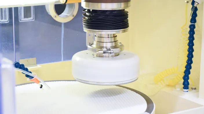
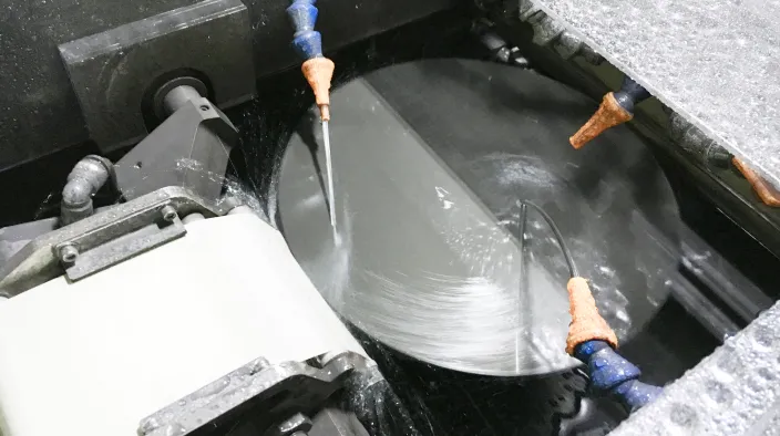
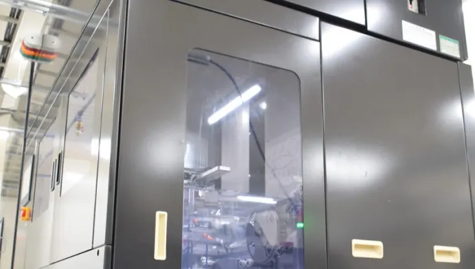
Processing Equipment List
| Equipment | Wafer Size (Inch) | Auto Type | Feature |
|---|---|---|---|
| Edge Polishing Machine | 18", 12" to 2", and Half Inch (SEMI standard sizes) |
Fully Automated | Polishing film method |
| CMP Equipment | 12" to 4" (Manual support for 3" and above) |
Semi-Automatic | Surface polishing |
| Single-Sided Lapping Machine | 6" to 2", Half Inch, and small chip sizes | Manual | Surface polishing |
| Single-Sided Grinding Machine | 12" to 2", Half Inch, and small chip sizes | Semi-Automatic | Surface grinding |
| Scrub-Type Wafer Cleaning Machine | 18" (450mm), 12" to 6" | Semi-Automatic | Brush cleaning |
| Megasonic Wafer Cleaning Machine | 6" to 2", and Half Inch | Manual | Ultrasonic bath cleaning |
| Wafer Dicing Machine (Size Reduction) | 12" to 2", and Half Inch | Manual | Laser and blade methods |
| Laser Marking Equipment | 12" to 2" | Manual | |
| Long Filler Bar Polishing Equipment | ー | Fully Automated | Superconductor wire polishing |
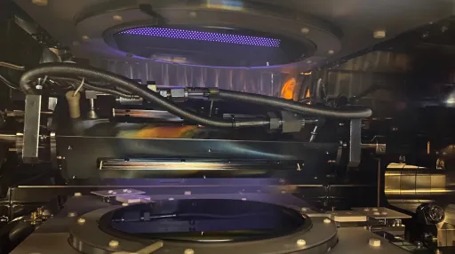
450mm Edge Polishing Equipment
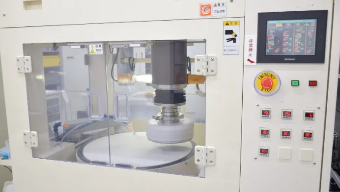
MAT CMP 200mm Surface Polishing Equipment
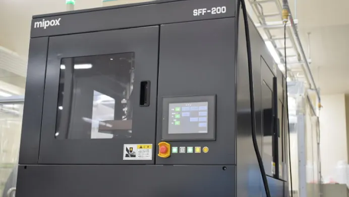
SFF-200TX Edge Polishing Equipment
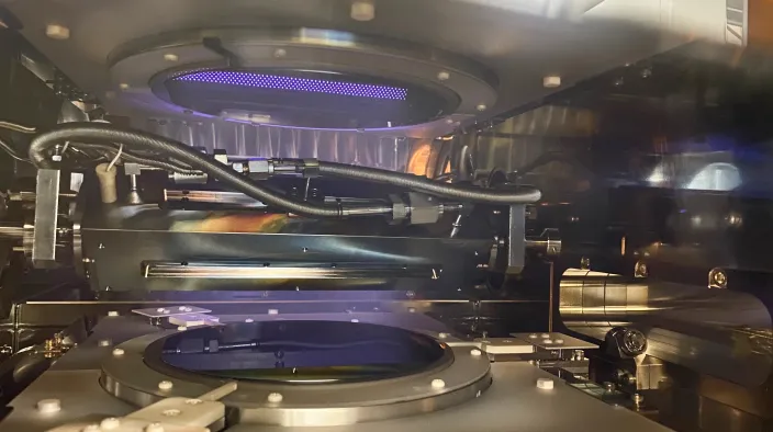
Inspection Equipment List
| Equipment | Wafer Size (Inch) | Auto Type | Feature |
|---|---|---|---|
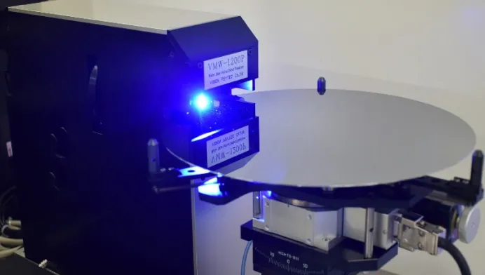
| Micro-Max VMW | 12" to 2", Half Inch, and small chip sizes | Manual | Wafer edge defect inspection |
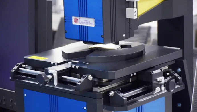
| Micro-Max VMX6100 | 8" to 2", Half Inch, and small chip sizes | Manual | Wafer surface defect inspection |
| Micro-Max XS-1 | 6" to 2", Half Inch, and small chip sizes | Manual | Transmission dislocation visualization |
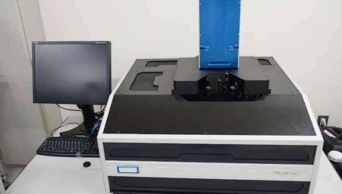
| VDM-5000 Ultima (Defect Inspection) | 4" | Manual | Automated wafer surface defect inspection |
| KLA-TENCOR P-10 | 12" (limited conditions), 8" to 2", Half Inch, and small chip sizes | Semi-Automatic | Stylus-type profiler |
| ZYGO NewView 7100 | 12" to 2", Half Inch, and small chip sizes | Semi-Automatic | Non-contact surface roughness and shape measurement |
| NANOSPEC AFT5000 | 12" to 2", Half Inch, and small chip sizes | Semi-Automatic | Optical interference film thickness measurement |
| Sheet Resistance Meter | 12" to 2", Half Inch, and small chip sizes | Manual | Metal thin film thickness measurement |
| NanoNavi L-trace Ⅱ | 8" to 2", Half Inch, and small chip sizes | Semi-Automatic | Atomic force microscope (surface roughness measurement) |
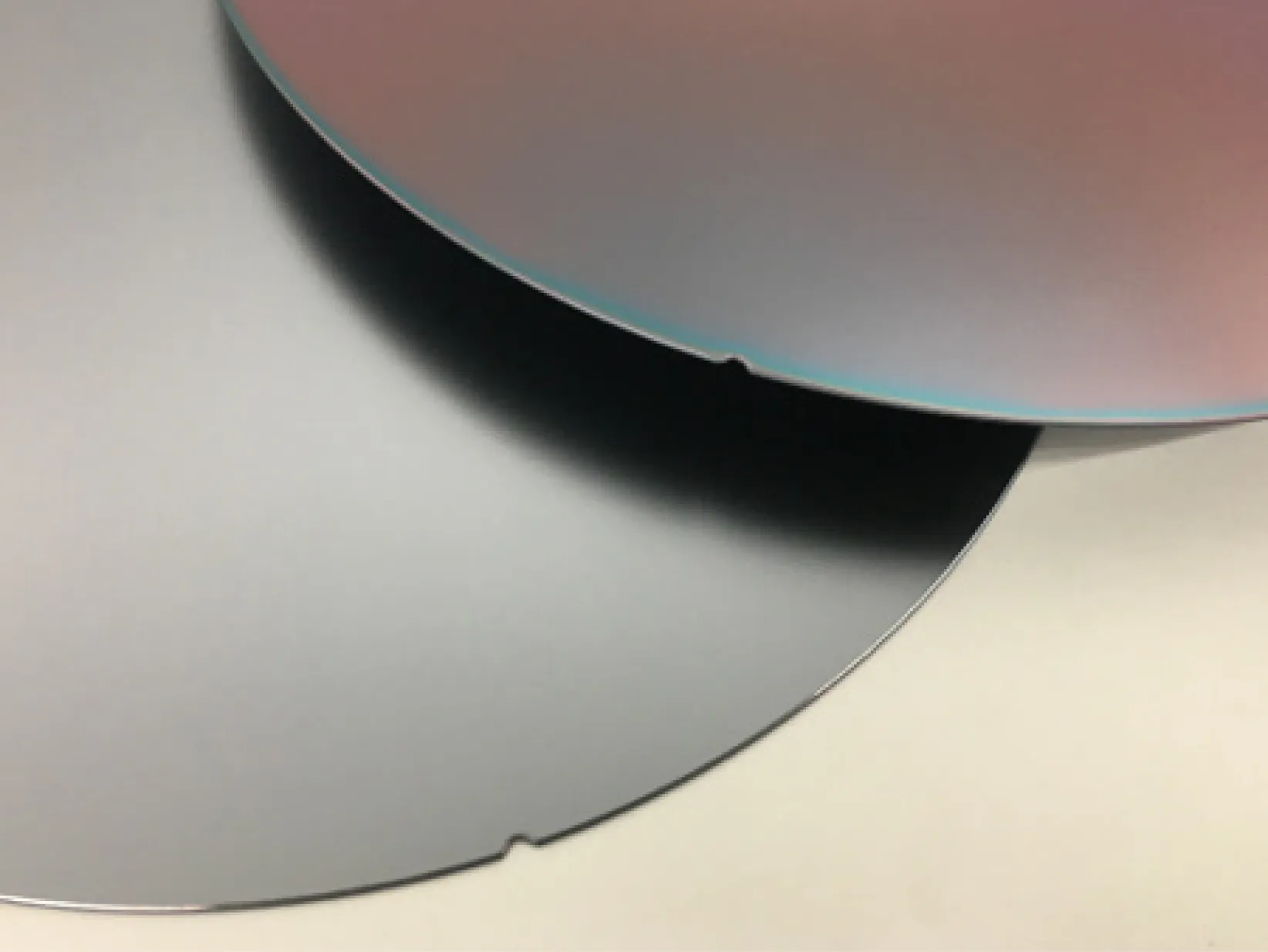
| Edge Profiler | 12" to 2", Half Inch, and small chip sizes | Manual | Edge shape measurement |
Micro Edge
Micro-Max XS-1
VDM-5000 Ultima
Inquiries about Precision Polishing Services
If you have any issues with precision polishing services, please feel free to consult us. Mipox, an expert in high-precision polishing, will propose solutions tailored to your challenges.
Q&A on Polishing Services
What types of polishing processes do you support?
We mainly handle edge polishing, planar polishing, and CMP.
Besides this, we also provide one-stop solution services that integrate multiple processes together, including resist coating (to protect the front and back surfaces of wafers), size reduction processing, and precision cleaning. Please feel free to contact us.
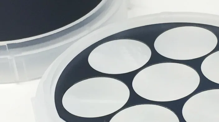
Are the wafer sizes you support determined?
We also handle special size wafers other than ASEMI standards. We flexibly handle square or chip-shaped substrates, fan-shaped, small, or half-inch pieces. Please consult us about your desired sizes and shapes.
What types of materials can be polished?
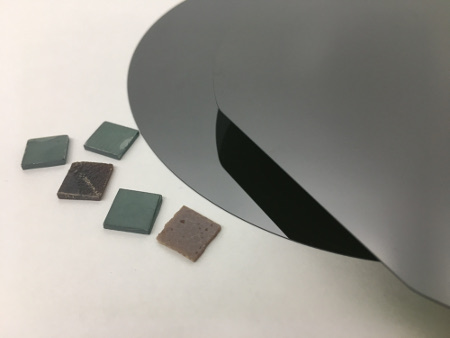
We have an extensive track record of polishing a wide range of materials - from silicon wafers at the top of our list to common materials such as compound semiconductors, oxide materials, and ceramics (Engineered Substrates), and also special materials such as organic crystals and composite materials.
See our track record of polishing here.
Can I receive a report on the results of a requested polishing service?
We provide appropriate documentation according to your requirements. Please consult us when considering specifications at the time of a project inquiry.
What are delivery times?
Delivery times vary depending on the requested content, quantity, difficulty level, and how many projects we are currently handling. Please refer to the following for normal turnaround times:
- Device wafer edge trimming: Within a few days after receiving wafers
- Ceramic substrate planar polishing: Approximately one to several weeks
- Wafer making from ingot: Approximately one to several months
Mipox Technology Polishing Process Examples
Silicon Wafers
Compound Semiconductor Materials (Next-Generation Semiconductor Materials)
Fine Ceramics (Polycrystalline, Sintered, and Composite) Materials
Effective Edge Polishing Film for GaNonSi Challenges
CONTACT
Mipox, the polishing professional, will propose the best polishing solutions, materials, and tools to meet your needs.
Please feel free to contact us.