Search by Solutions
Product
Search
Edge and Notch Polishing Service
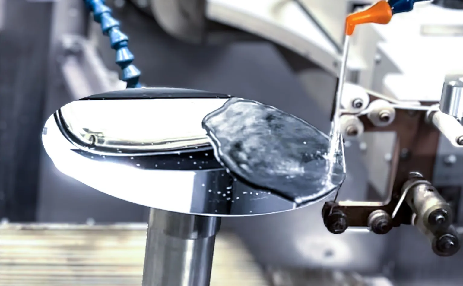
Polishing Film Type Edge Polishing
Mipox provides its proprietary edge and notch polishing service using a "polishing film", which is an abrasive product manufactured in-house, along with "dedicated edge and notch polishing equipment".
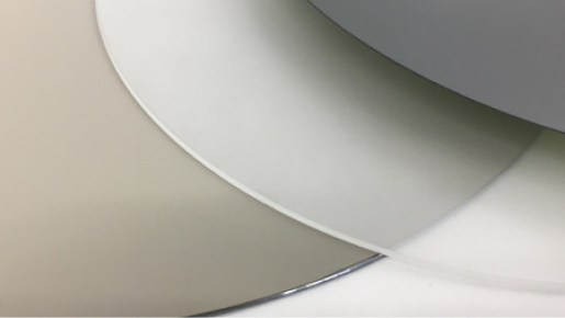
To say nothing of semiconductor wafers (SEMI standard products), Mipox flexibly supports special format size wafers, glass substrates, bonded composite wafers, and others as well.
Since we have extensive experience also with SiC, GaN, and diamond, which are typical difficult-to-machine materials, as well as oxide materials and ceramic materials, we can respond to diverse requirements.
- Wafer Polishing Process
- Edge Polishing and Chamfering
- Edge Trimming
- Membrane Removal
- Cleaning Process
- Compound Semiconductor Chamfering
- Terrace Forming and Polishing
- Non-standard Size Chamfering
- Alignment Correction
- 8-inch SiC wafer
- Cost Example
Wafer Polishing Process
Slicing
Cut the ingot.
Beveling
Adjust the diameter dimension. Perform chamfering and damage prevention.
Lapping
Grind both surfaces of the wafer to adjust the thickness. Remove waviness.
Etching / Heat Treatment
Remove altered layers. Create wafers with electrical characteristics fit for their applications.
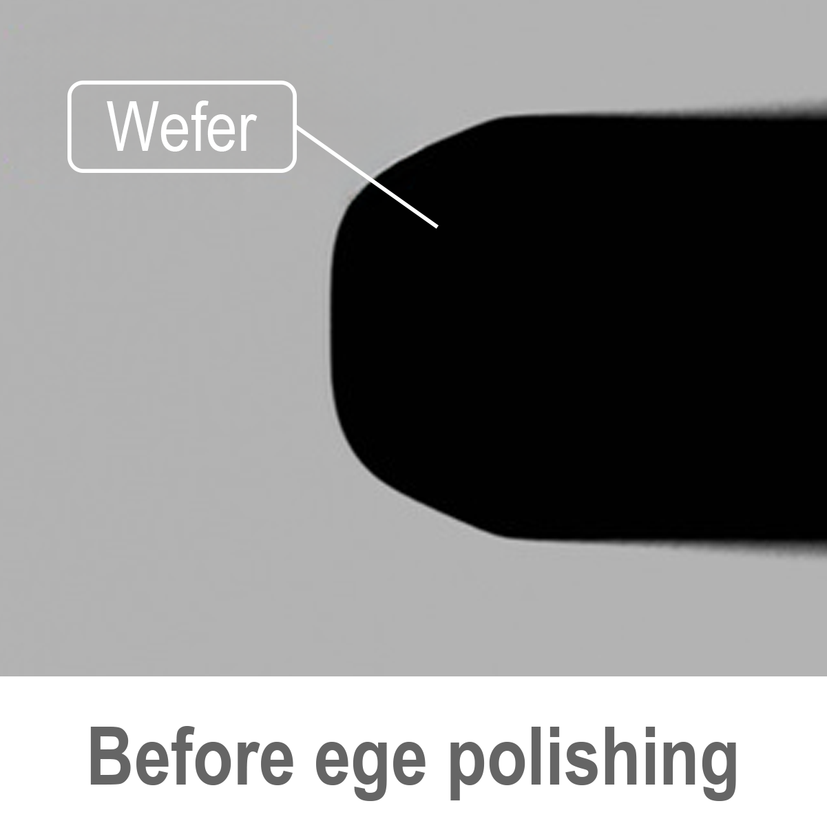
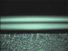
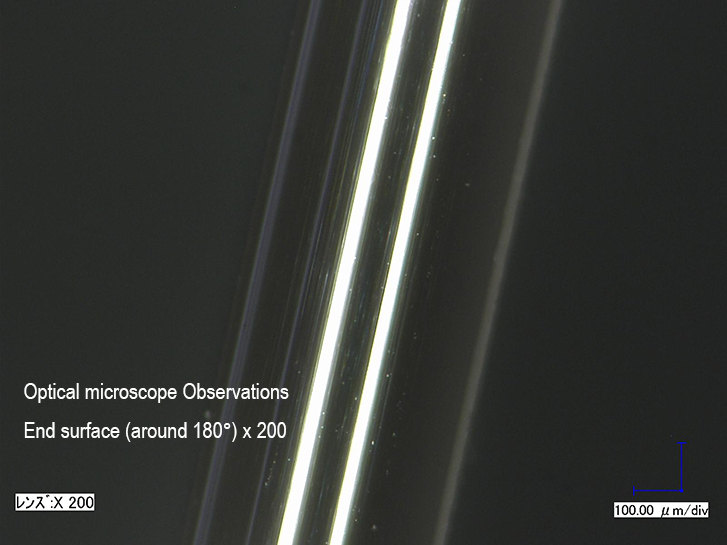
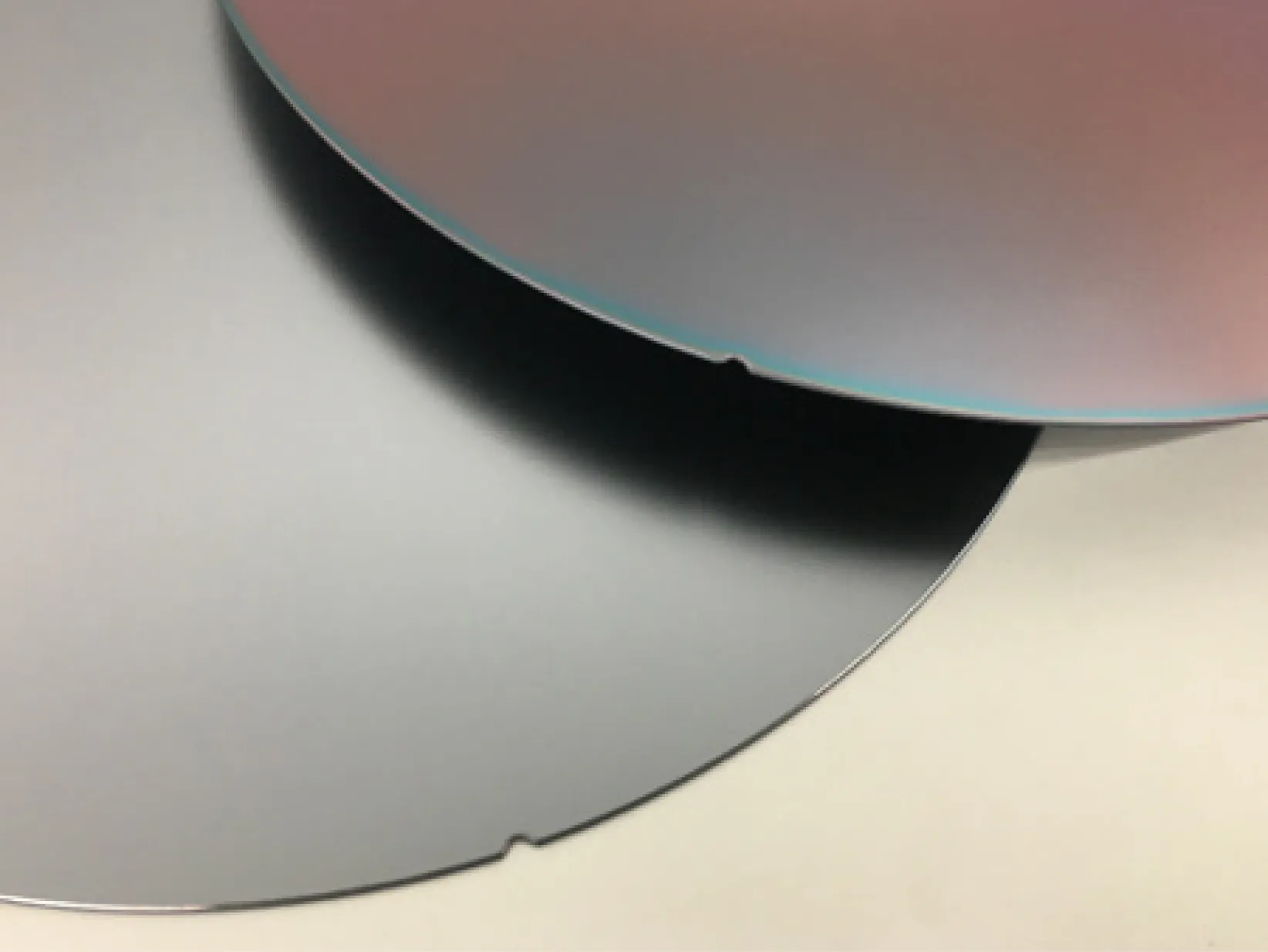
Edge / Notch polishing
Mirror-finish edge and notch areas.
Surface polishing
Remove surface irregularities and flatten the surface.
Cleaning / Inspection
Leveraging a polishing film's characteristics of "flexibility" and "continuous cutting edge (grit) switching", we developed a high-efficiency process in house that achieves both low damage to wafers and high polishing rates and are expanding it to our polishing service. Depending on the selected polishing film, we can easily handle difficult-to-machine materials like SiC and GaN.
Moreover, our polishing service is often utilized not only in wafer manufacturing processes but also in semiconductor "post-processing" applications. Particularly, our independently developed "Edge Trimming Process" designed to prevent wafer damage during backgrinding (BG) is a key application characterized by its ability to remove a wafer and BG tape simultaneously. (Japanese Patent No. 4463326)
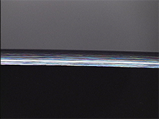
Edge Polishing and Chamfering
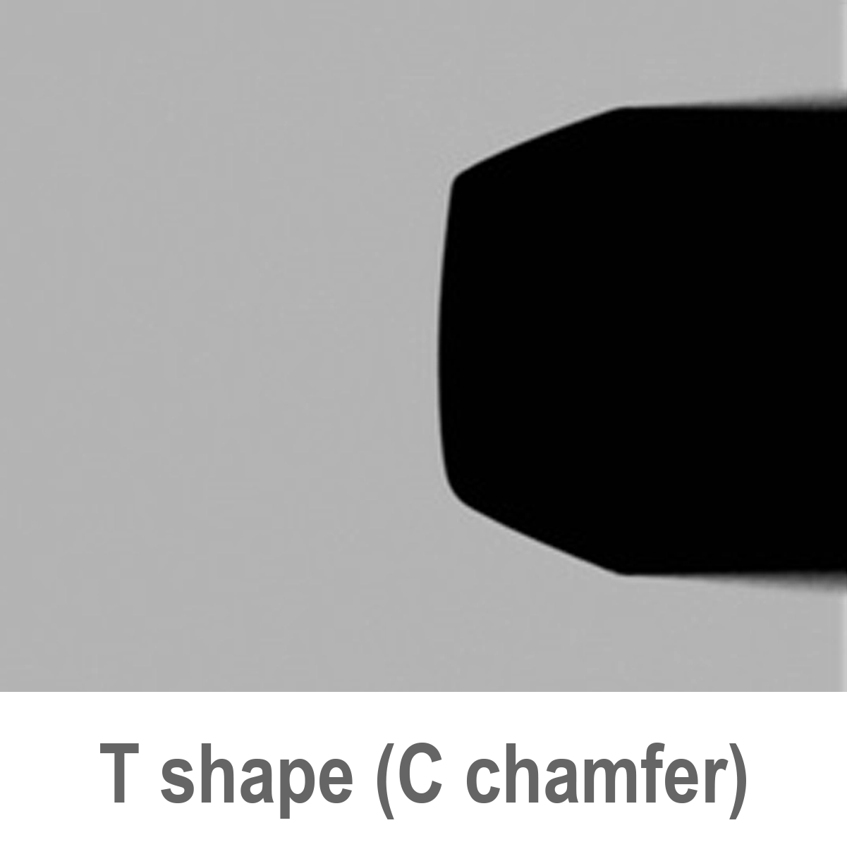
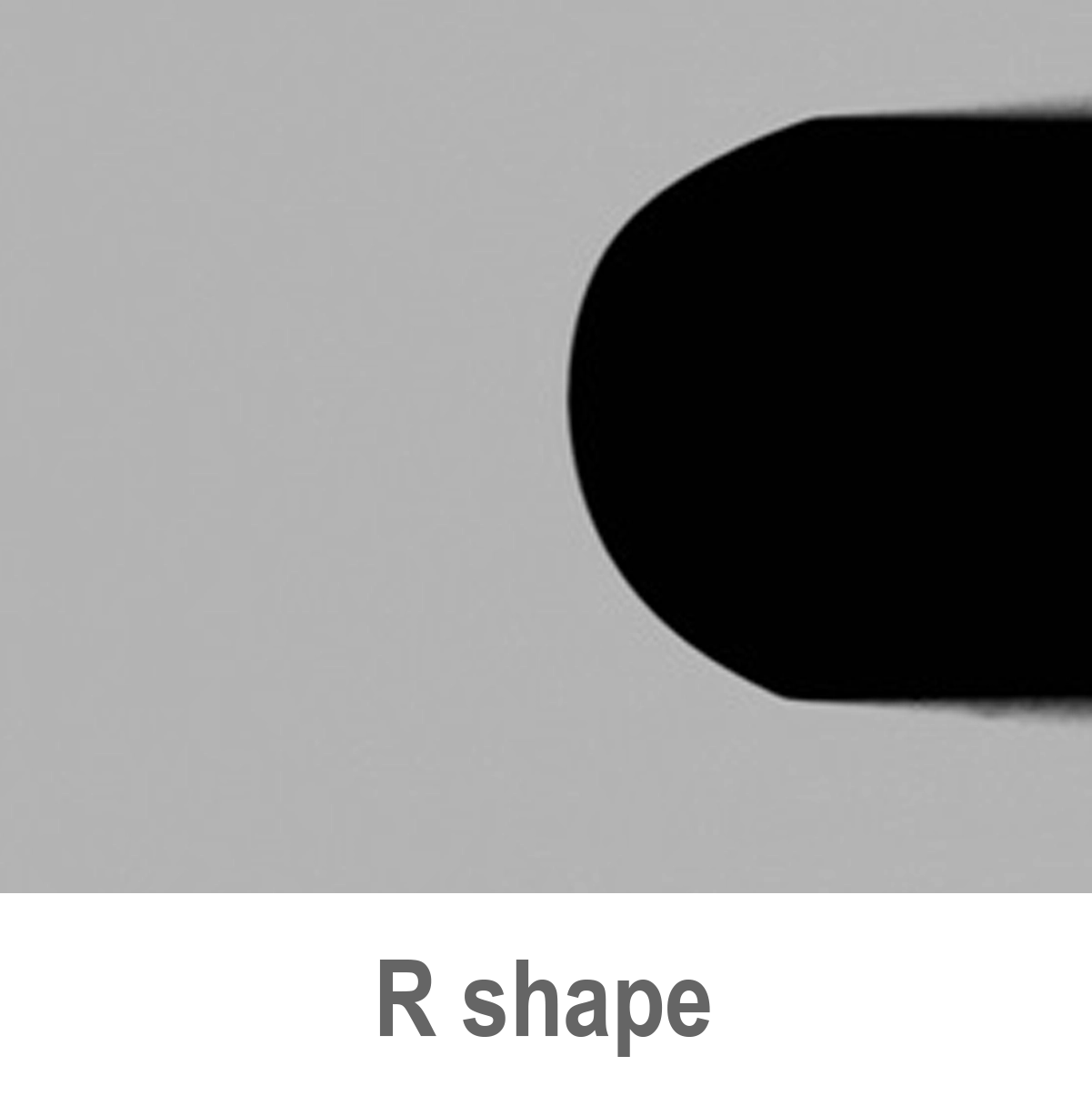
Mipox's edge polishing service (polishing film type edge polishing) also supports difficult-to-machine materials, which are difficult to handle using other methods such as the abrasive grinding or slurry polishing methods. We will finish edge shapes and edge/notch surface roughness according to your desired shape and precision.
Film Polishing Method Strengths & Features
Supports high variety and low volume products. Edge shapes can be modified flexibly.
Edge shapes for high variety and low volume products can be modified based on the conditions (recipe) for the polishing equipment. Unlike general abrasive grinding methods, there is no need to prepare grindstones fit for each edge shape. We can flexibly respond to needs for high variety and low volume edge shapes.


Possible to modify and adjust edge and notch surface roughness easily by changing polishing film types (selecting).
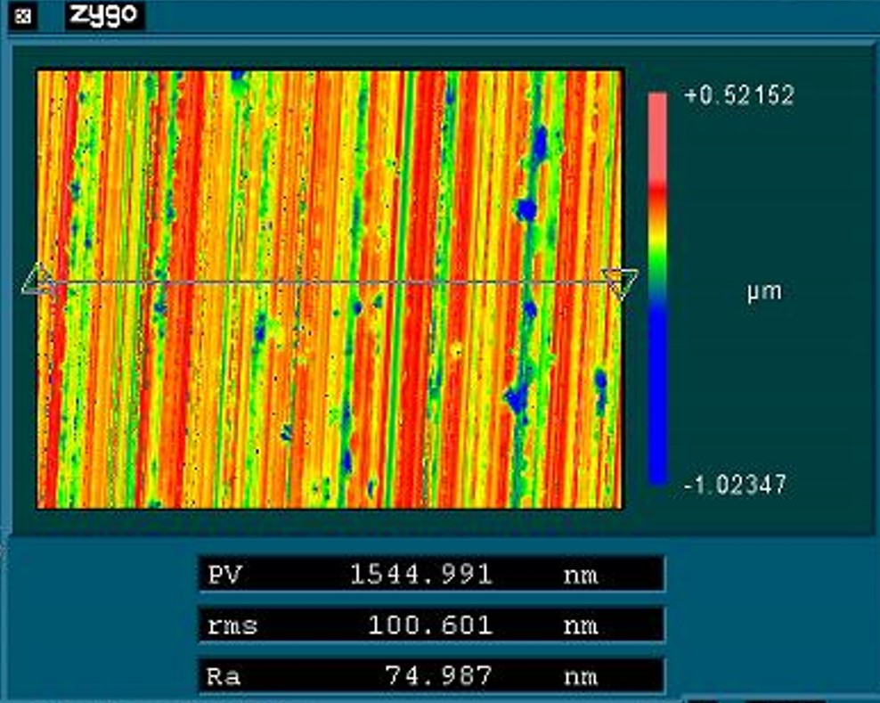
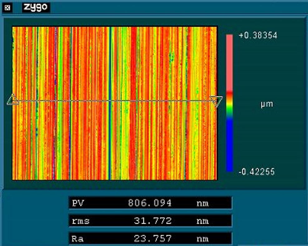
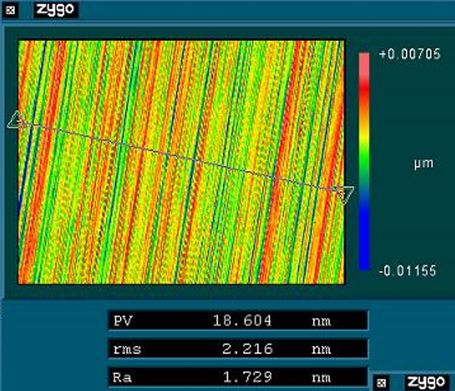
Mirror finishing up to 10nm can be achieved by repeating polishing.
Significantly reduces chipping (microscopic chipped pieces, cracks) when compared to other abrasive griding methods, and can also be applied to delicate template substrates like GaNonSi.
Does not use liquid chemicals (acids, alkalis) during edge polishing, which saves you the trouble of cleaning wafers, processing waste liquid, and others.
Achieves 3 to 5 times higher chamfering efficiency compared to abrasive grinding methods for difficult-to-machine materials like SiC and GaN.
Possible to polish also resin and metal materials (Cu membrane, Au membrane), materials that abrasive grinding methods are not good at polishing, without problem.
Edge Trimming
Preventing Edge Area Damage During Wafer Thinning Process
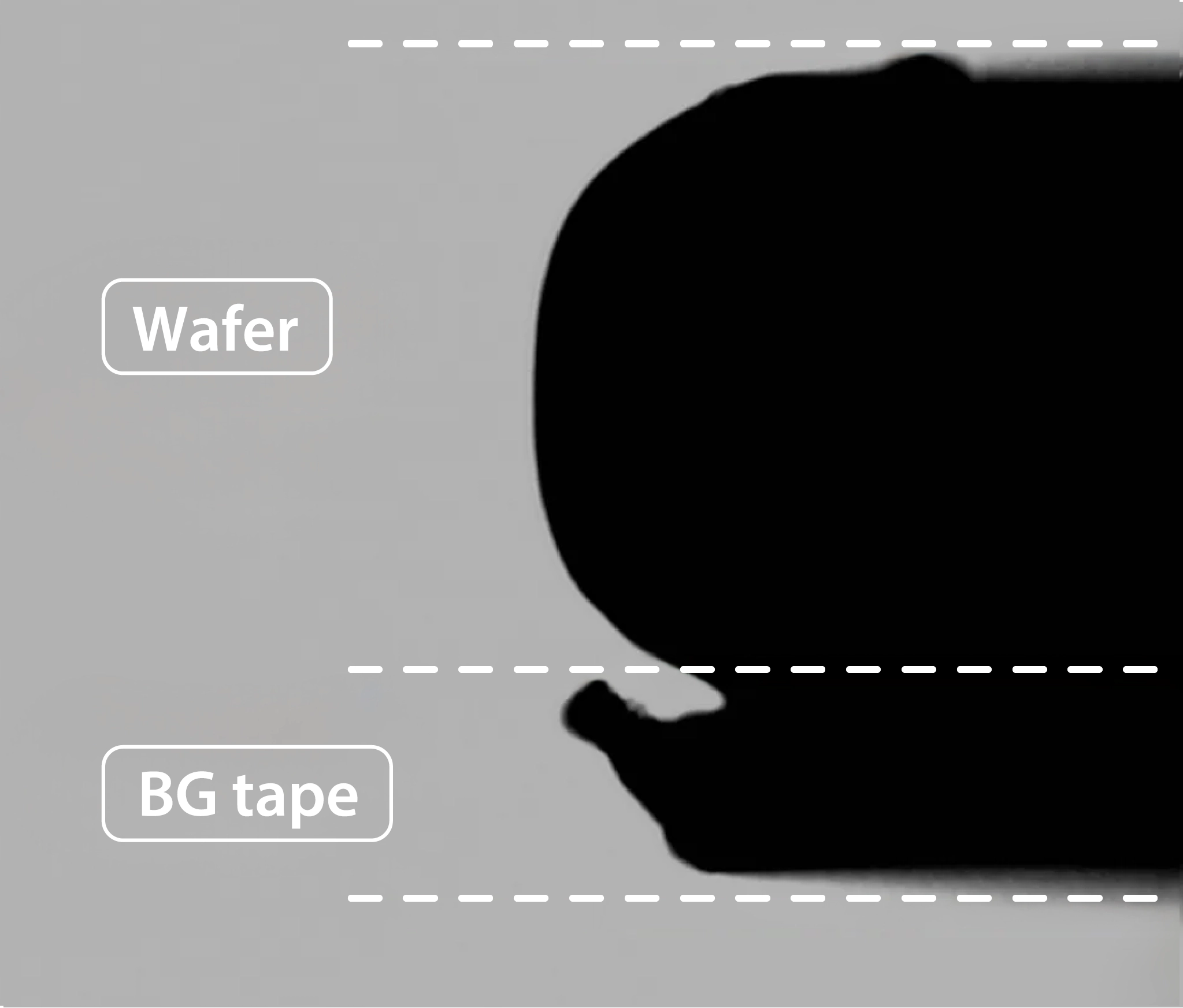
General backgrinding (BG) situation without edge trimming
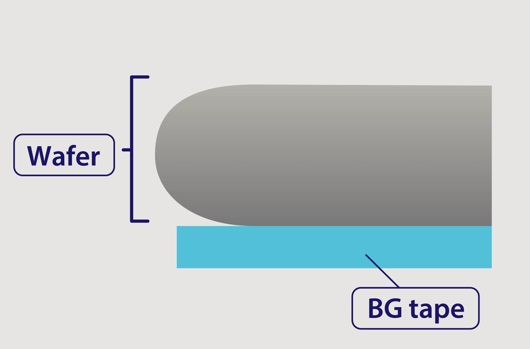
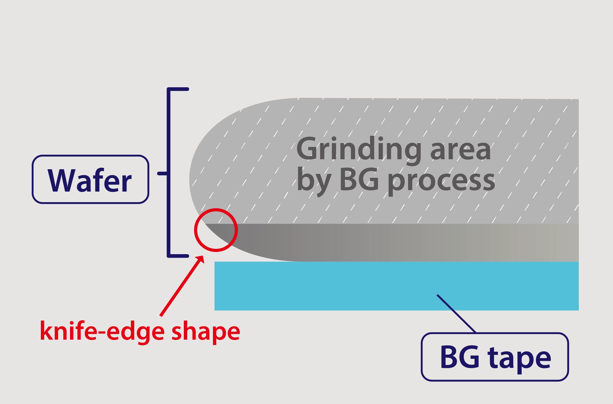
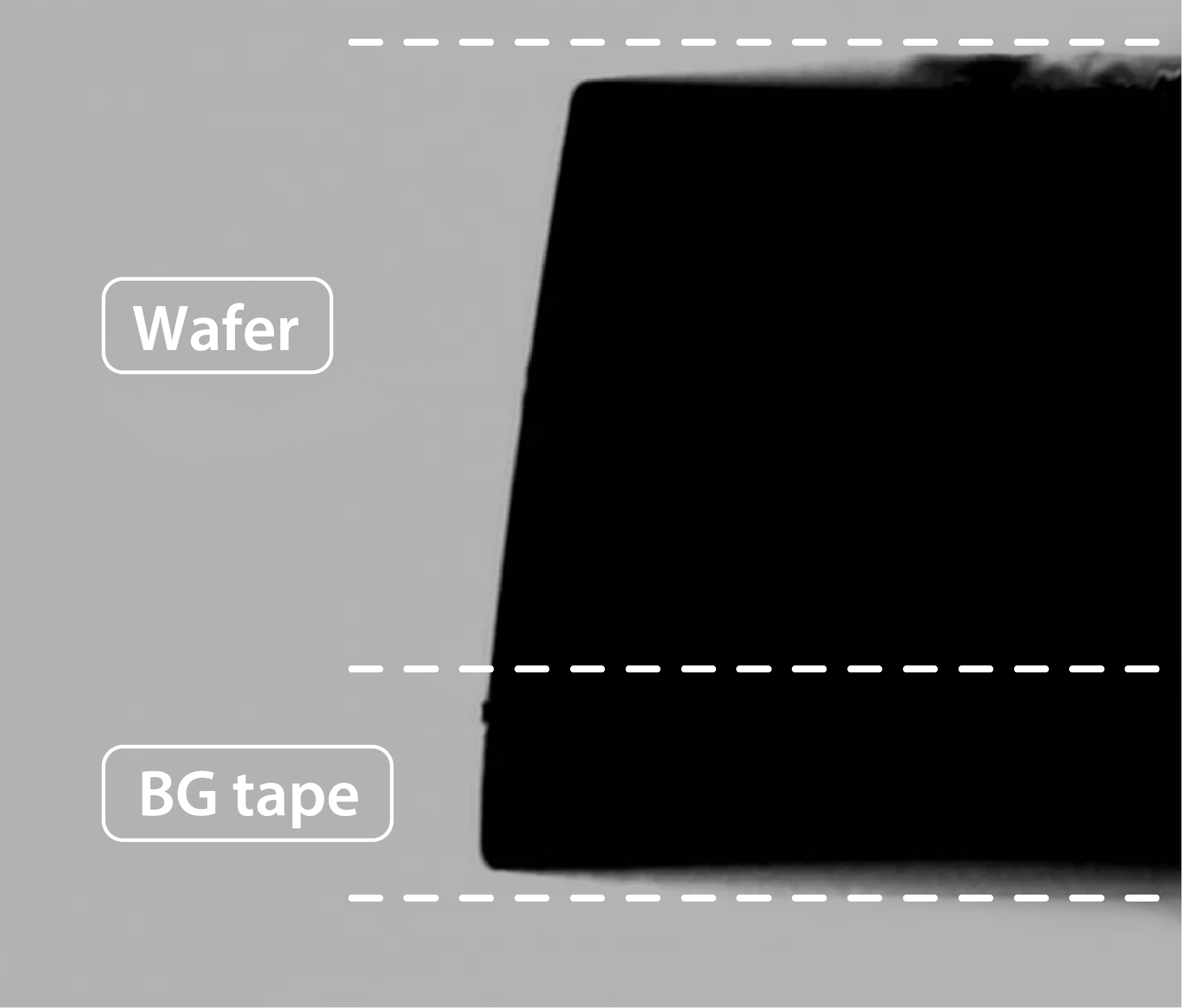
State of edge trimming using a polishing film method
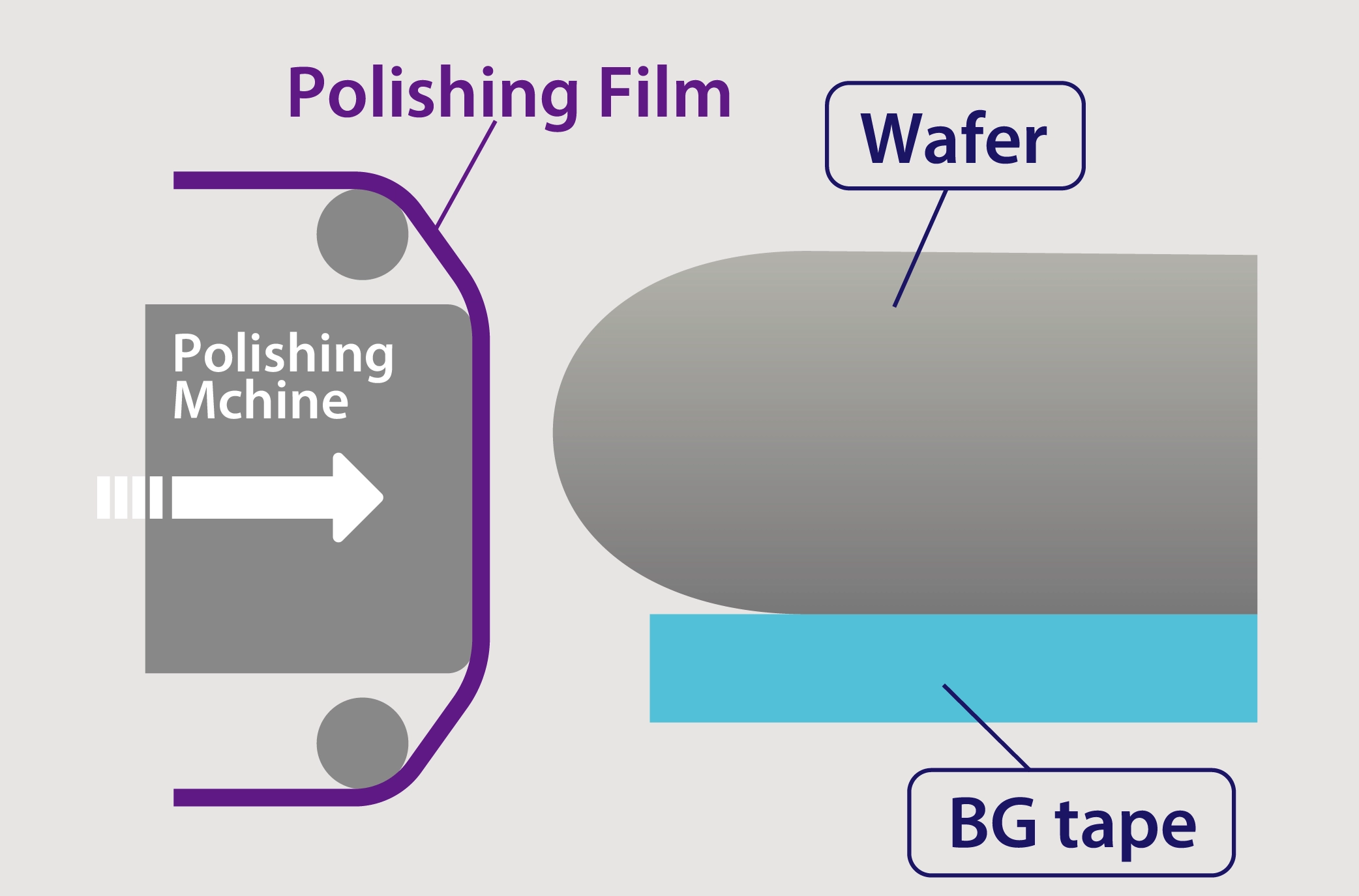

Mipox's edge trimming service (polishing film type edge trimming) is effective at improving yield in backgrinding processes (BG) for semiconductor wafers.
It helps perform stable edge trimming without being affected by resin membranes, metal membranes (Cu, Au), and others existing in edge areas. Additionally, this processing can be applied "after attaching BG tape" because both the BG tape and wafer can be trimmed at the same time. For that reason, without modifying the existing processes, trimming (process) can be introduced easily.
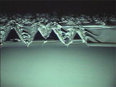
Reclaimed Wafer Applications - Edge/Notch Membrane Removal
The edge/notch polishing service (polishing film type edge and notch polishing) can efficiently remove unwanted membranes and defects while keeping wafer diameter reduction to a minimum. Taking advantage of this characteristic, we have achieved a good track record of adoption of this service for wafer reclamation applications (reclaimed wafer market).
Even for such wafers as those with carbon-based membranes for which removing membranes by chemical etching is considered to be difficult and those in an abnormal state with large irregularities, their appropriate edge quality can be restored without difficulty.
For large diameter SiC (8-inch) wafers as well, including edge and notch areas, this service supports reclamation polishing applications (polishing for the purpose of reclamation).
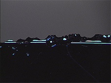
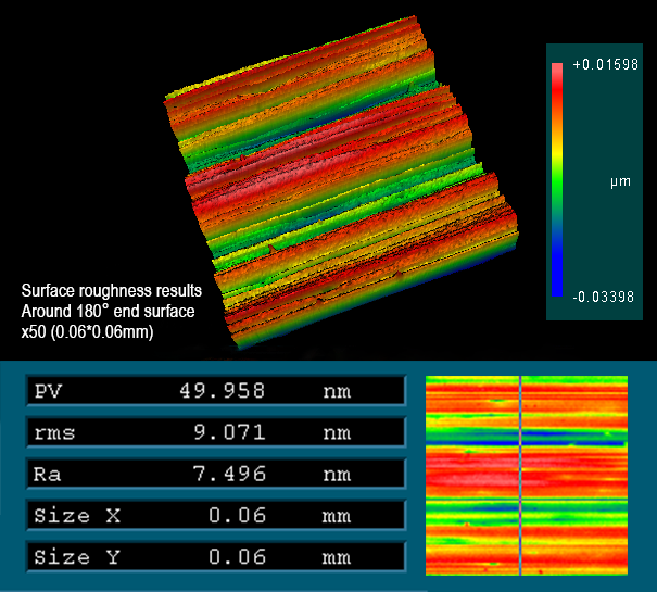
State of edge (notch) before polishing Example:
Roughness at edge in etching process
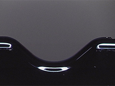
State after polishing film type edge polishing
(after rough polishing process)
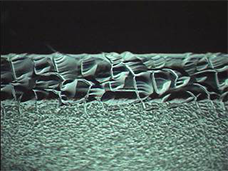
State of edge (notch) before polishing Example
Abnormal crystal growth at edge during epitaxial film growth

State after polishing film type edge polishing
(after finish polishing)
Edge/Notch Cleaning Process
Mipox's edge and notch polishing service (polishing film type edge polishing) can solve the problem of resin (adhesive) adherence on edge areas that can occur during composite wafer manufacturing or processing using high-bump backgrinding tape.
Unlike abrasive grinding and slurry methods, one of the characteristics of the polishing film type method is that it is not likely to be affected by causes such as clogging due to the physical properties of the polishing target. By applying a dedicated cleaning film, it is possible to remove resin material (such as an adhesive) adhering to the edge and notch areas effectively.
This cleaning process is an application specific to the polishing film type method that contributes to yield improvement particularly in the backgriding process (BG).
Before edge trimming process
After edge trimming process
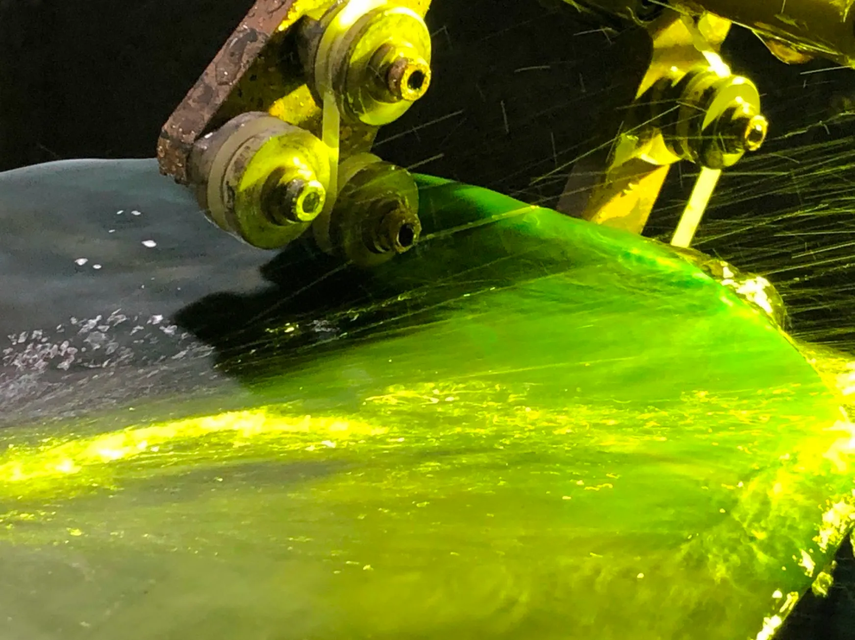
Compound Semiconductor and Oxide Material Chamfering and Mirror Finishing
Mipox's edge and notch polishing service (polishing film type edge polishing) is recognized as causing less damage to wafers than other methods and is often used for chamfering for compound semiconductor wafers such as SiC and GaN.
Chamfering by the polishing film type method is particularly compatible with a water assisted laser cutting method and is getting attention as the only method that can rationally achieve the addition of chamfering after hollowing from a base material (coring) or for resizing applications. We have received many inquiries especially for large diameter to 8-inch SiC wafer applications and ceramic material wafer fabrication applications.
Roughness of oxide semiconductors after polishing
Edge observation of oxide semiconductors: perfect mirror surface achieved
Top Edge Polishing and Terrace Formation Polishing
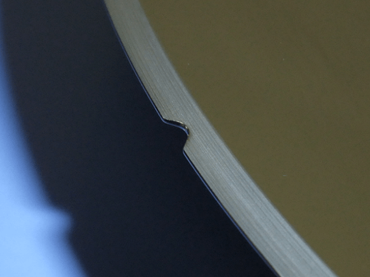
For template wafers of GaNonSi (SiConSi9), GaNonSiC, and others, it is known that wafers are likely to be broken due to the difference in physical properties between the bulk and epitaxial layers. If some defects exist at the edges, the risk of damage to the entire wafer including the bulk increases, and even if that damage does not lead to breakage, the risk of the occurrence of fatal damage such as slip in the surface membrane (surface area formed by the heteroepitaxial growth) increases as well. Removing such defects in advance is very important.
Our top edge polishing (terrace formation polishing) using the polishing film type method reduces load on both the bulk and epitaxial layers and removes defects at the edges. Even a mirror surface can be achieved. This is one of the unique applications of the polishing film method that cannot be handled by abrasive grinding or slurry polishing methods.
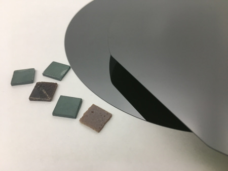
Chip-Shaped and Non-Standard Size Wafer Chamfering
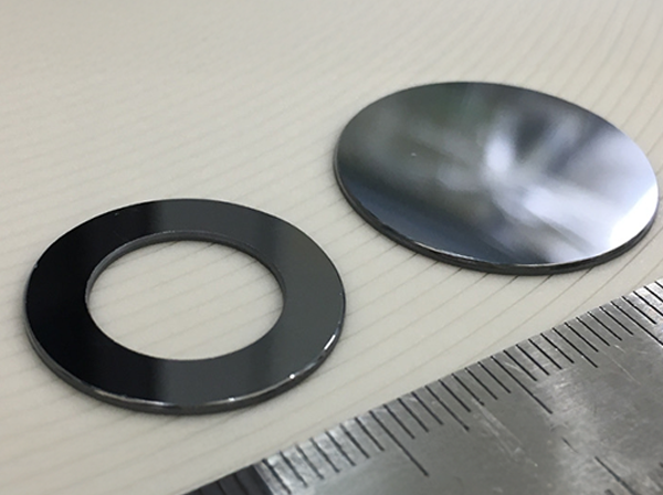

Mipox's edge polishing service (polishing film type edge polishing) also handles chip-shaped (square) wafers used for research and development applications, and others and for special small-diameter wafers (half-inch size) of 1 inch or less in diameter.
Normally, chip-shaped (square) wafers have sharp corners and edges. They may cause breakage or damage (edges dropping off) during such processes as planar polishing. Chamfering, which can eliminate the causes of the above in advance, is very important.
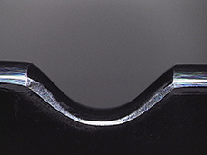
Wafer Bonding Alignment Correction
When two wafers of different materials are bonded, if misalignment occurs and causes edge protrusion, an almost perfect circular shape can be restored by polishing the relevant edge intensively.
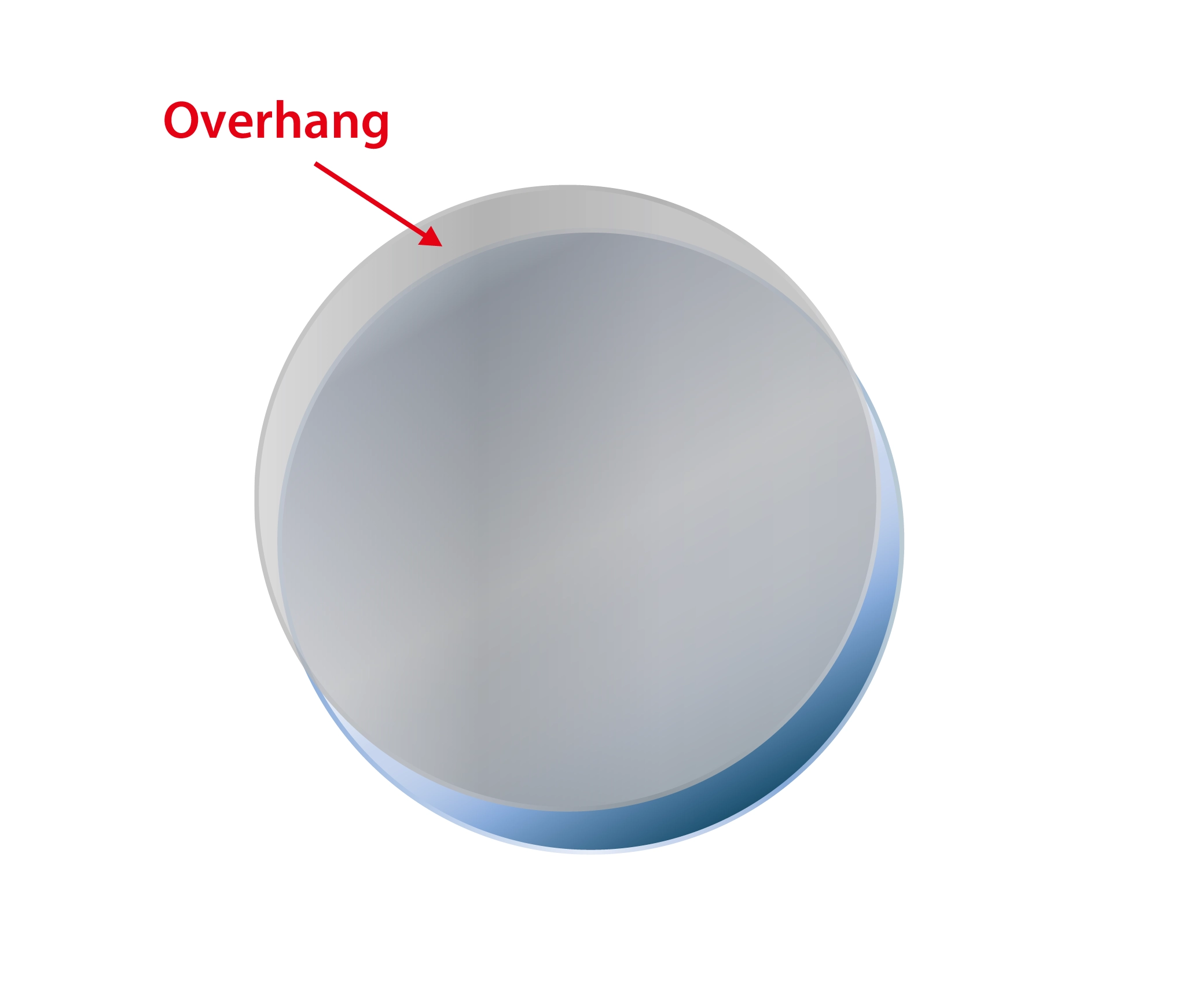
Wafer that has been misaligned during the bonding process (before edge polishing)
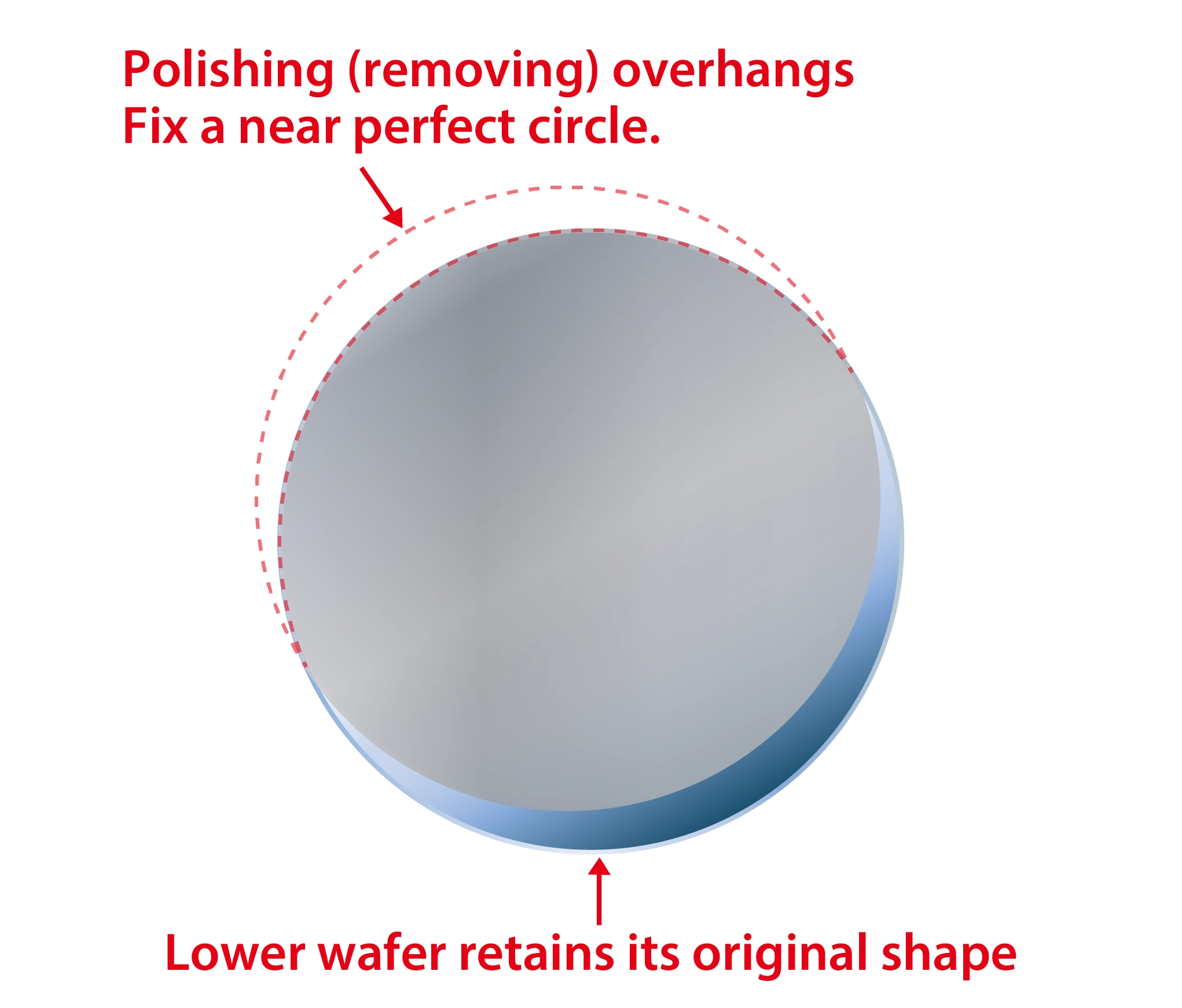
Wafer with misalignment corrected in the bonding process (after Mipox edge polishing)
Large Diameter 8-inch SiC (Silicon Carbide) Wafer Notch and Edge Chamferring
Mipox established a method that can perform stable chamfering for large diameter 8-inch SiC wafers, which are regarded as a key material among next generation power semiconductor materials.
Mipox provides polishing services and notch/edge polishing equipment with dedicated specifications specializing in 8-inch SiC wafer applications.
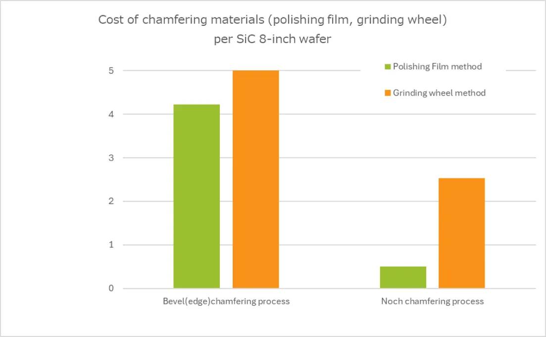
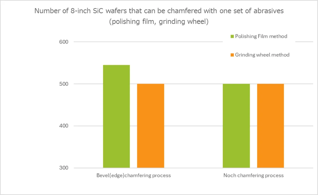
Cost example (for single crystal 8-inch SiC wafers) Polishing film type chamfering
Chamfering by the polishing film method has a higher cost performance than other methods, especially for difficult-to-machine material applications.
The cost of chamfering for crystal 8-inch wafer applications (a comparison between chamfering using an abrasive film and chamfering by an abrasive grinding method) is shown in a separate graph.
For the polishing film method, chamfering can be performed at a low cost. For the chamfering of notches, in particular, its cost is approximately 1/5 the cost required by the abrasive grinding method - overwhelmingly low. In addition, the polishing film method is also superior in terms of the operation ratio because equipment downtime required for such work as changing abrasive materials can be kept short.
Mipox Technology Polishing Process Examples
Silicon Wafers
Compound Semiconductor Materials (Next-Generation Semiconductor Materials)
Fine Ceramics (Polycrystalline, Sintered, and Composite) Materials
Effective Edge Polishing Film for GaNonSi Challenges
CONTACT
Mipox, the polishing professional, will propose the best polishing solutions, materials, and tools to meet your needs.
Please feel free to contact us.