Search by Solutions
Product
Search
Large Diameter 8-inch SiC Wafer Notch and Edge Chamferring

Providing Rational Notch and Edge Chamfering Applications
Mipox achieves stable chamfering processing of 8-inch SiC wafers through its proprietary polishing films and equipment. We flexibly provide services from sample processing to mass production according to your requirements.
The polishing film method, which combines low damage with high efficiency, has been particularly well-received as a rational process showing high processing efficiency for notch area chamfering.
Flexible polishing services are available from sample processing to small-lot and mass production according to customer requirements.
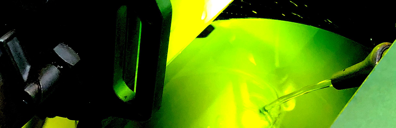
Edge Polishing Process Using Polishing Films
SiC is a difficult-to-machine material with hardness ranking after diamond and boron carbide. Therefore, conventional grinding wheel methods struggled to achieve adequate productivity, and faced significant issues particularly with notch area chamfering due to grinding wheel shape constraints and severe wheel wear preventing continuous grinding.
Mipox has solved these problems by applying proprietary polishing films and specialized chamfering equipment, establishing a rational chamfering method that achieves high productivity.
Advantages of the Polishing Film Method
Enables continuous chamfering without concern for abrasive wear. Minimal variation between wafers.
Can follow pre-cut notch shapes, enabling chamfering without distorting the original form. Highly compatible with laser cutting methods.
Approximately 5x higher throughput (processing capacity, processing speed) compared to grinding wheel methods. (*According to company research, May 2024)
Chamfering process follows crystal orientation properties inherent to SiC materials. Less likely to cause crystal structure-derived processing strain.
Due to constant pressure polishing mechanism, less likely to cause cleavage damage from notch.
No special chemicals or utilities required for processing, and no special utilities like laser processing needed. Therefore, fewer location restrictions for installation.
Clean specifications (with cleaning system) available. Can accommodate equipment configurations that suppress particle adhesion, resulting in fewer constraints on subsequent processes.
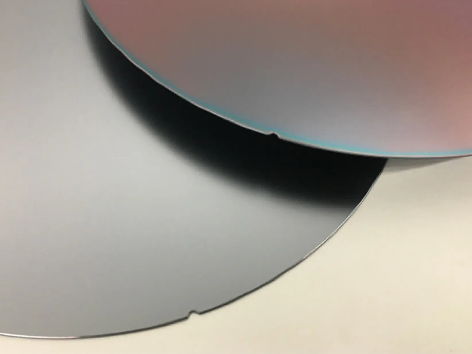
Before Notching
Notching Process
Slicing Process

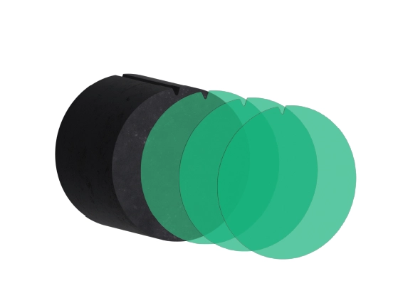
Chamfering
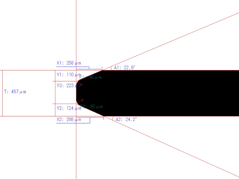
SiC Wafer Notch Chamfering
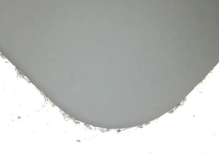
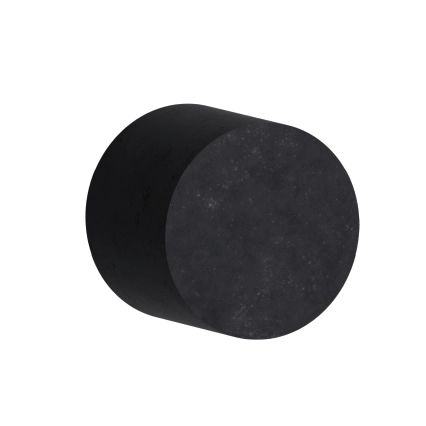
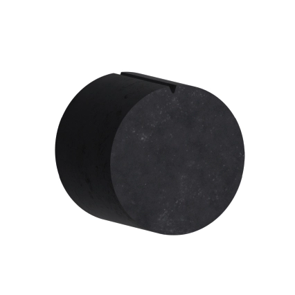
Before Chamfering
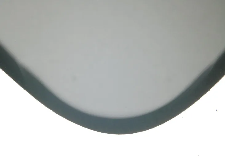
After Chamfering
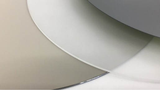
SiC Wafer Edge (Periphery) Chamfering
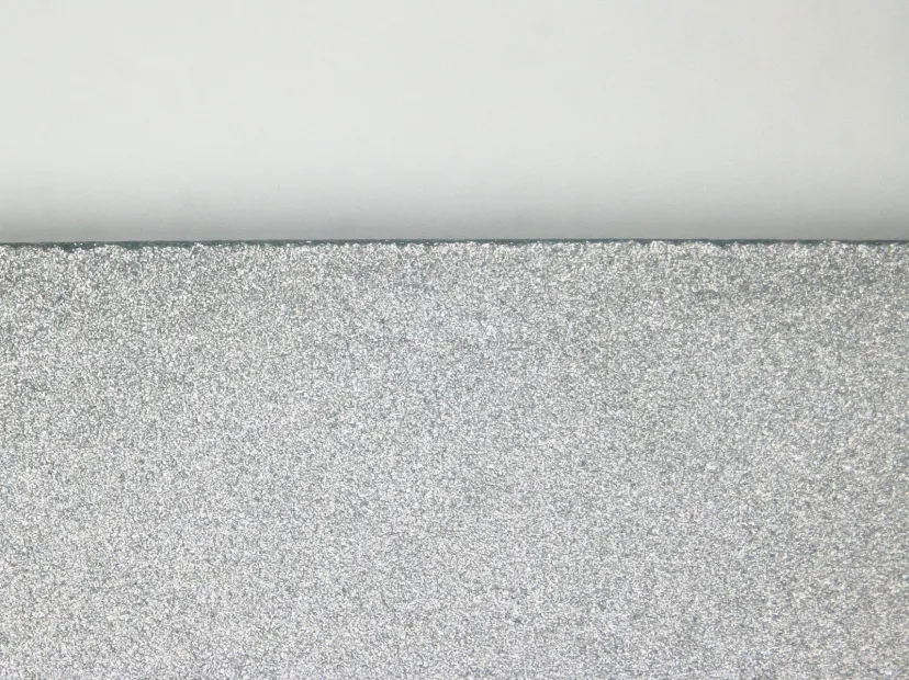

Before Chamfering
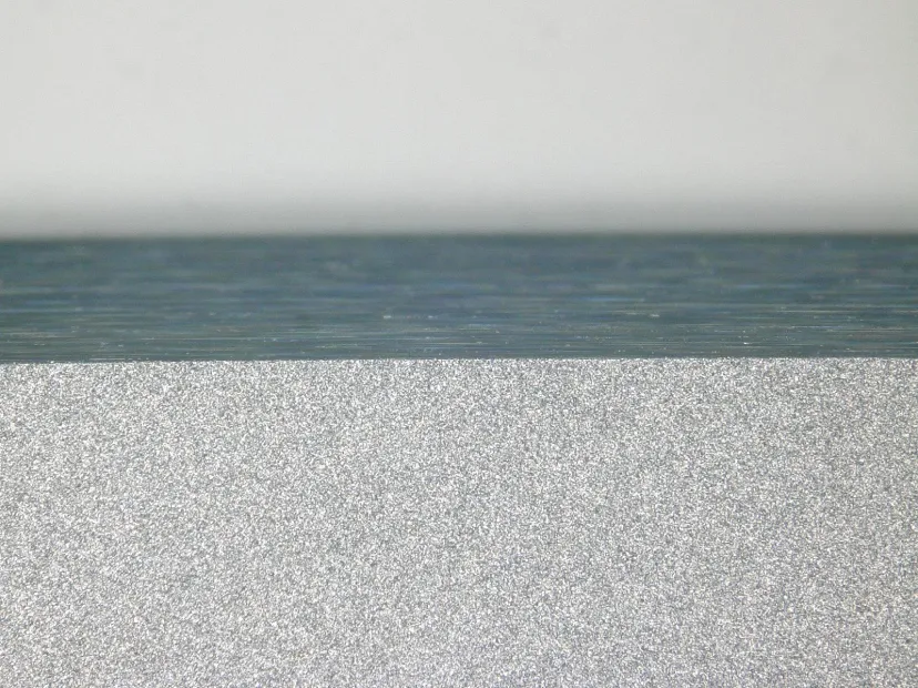
After Chamfering (Rough/Fine Chamfering)
Inquiries about Precision Polishing Services
If you have any issues with precision polishing services, please feel free to consult us. Mipox, an expert in high-precision polishing, will propose solutions tailored to your challenges.
Mipox Technology Polishing Process Examples
Silicon Wafers
Compound Semiconductor Materials (Next-Generation Semiconductor Materials)
Fine Ceramics (Polycrystalline, Sintered, and Composite) Materials

Effective Edge Polishing Film for GaNonSi Challenges
CONTACT
Mipox, the polishing professional, will propose the best polishing solutions, materials, and tools to meet your needs.
Please feel free to contact us.