Search by Solutions
Product
Search
Template Substrate Applications
Requirements for Template Substrate Processing
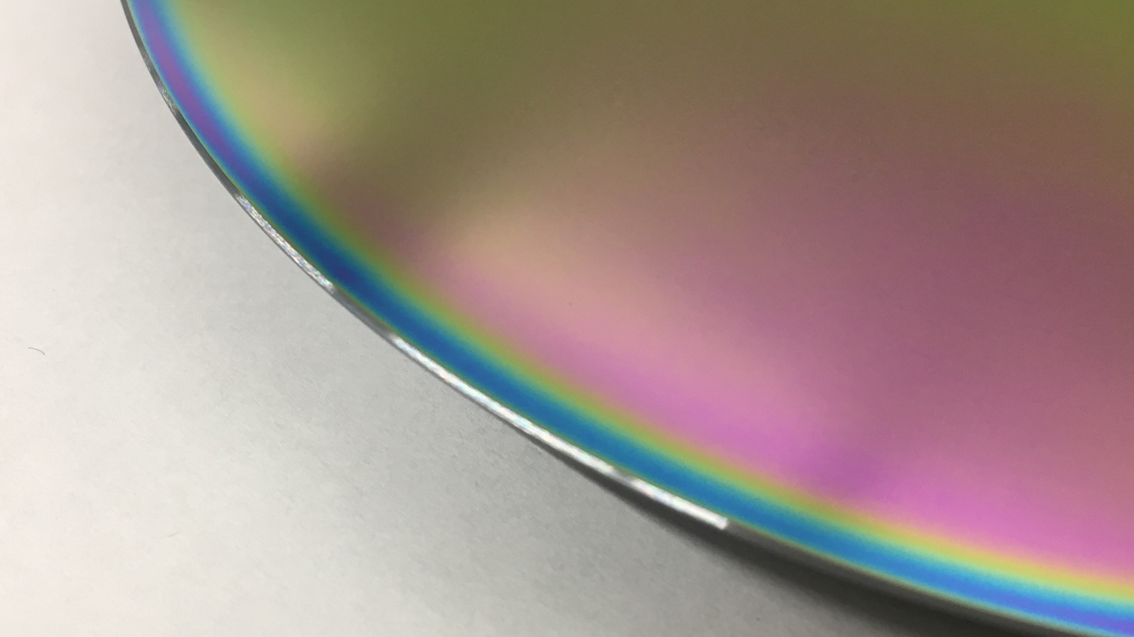
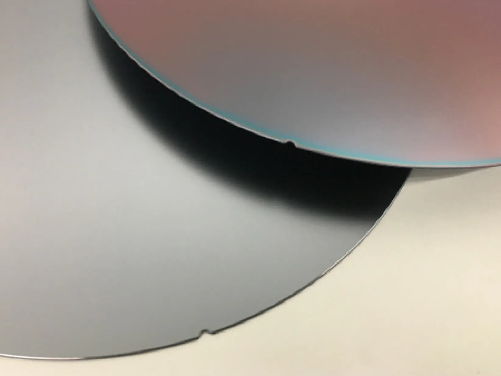
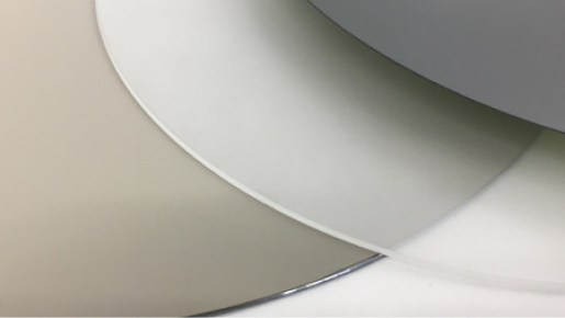
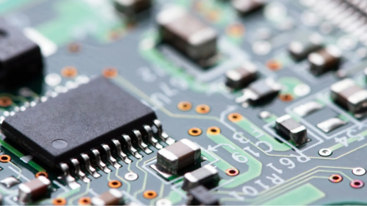
Template substrates, such as SiC-on-Si, GaN-on-Si, and GaN-on-SiC, which feature heteroepitaxial growth of materials like GaN or SiC on base wafers, are garnering significant attention in the industry. These substrates offer numerous advantages, including easier scaling to larger diameters, substantial cost reductions in LED and power semiconductor manufacturing, and compatibility with existing Si device production lines. However, to fully realize these benefits, it is crucial to remove the epitaxial film adhered to the edge of the template substrate.
Template substrates are particularly susceptible to wafer breakage due to edge defects. By preemptively removing these defects, significant yield improvements can be achieved. Mipox's contract polishing service employs an abrasive film-based edge film removal process that minimizes stress on the delicate epitaxial layer of various template substrates. This process exposes the underlying substrate and removes the diffusion layer, resulting in compound semiconductor wafers that can be processed in existing Si device manufacturing lines without contamination.
Materials :
GaN-on-Si, GaN-on-SiC, SiC-on-Si, SiC-on-SiC, etc.
Related Articles
Silicon Wafers
Compound Semiconductor Materials (Next-Generation Semiconductor Materials)
Fine Ceramics (Polycrystalline, Sintered, and Composite) Materials
Effective Edge Polishing Film for GaNonSi Challenges
CONTACT
Mipox, the polishing professional, will propose the best polishing solutions, materials, and tools to meet your needs.
Please feel free to contact us.